Advertisements
Advertisements
Question
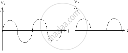
With the help of neat labelled circuit diagram explain the working of half wave rectifier using semiconductor diode. Draw the input and output waveforms.
Advertisements
Solution
A device which converts A.C. to D.C. is called rectifier. In this case output exists only for half cycle hence it is called half wave rectifier. Construction: The circuit diagram of a half wave rectifier using a junctiondiode is as shown in fig. The alternating voltage source is connected to the primary coil of a transformer. The secondary coil is connected to the diode in series with a resistance RL called the load resistance
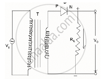
T=Transformer
D=Diode
V0=output voltage
v1=input votage
RL=load resistance
Working: In first cycle of input voltage, the anode of the diode is positive potential w.r.t. cathode. Hence the diode is in forward-biased. Hence it conduct current. The current flows through load resistance giving voltage drop iRL. This voltage drop is called output voltage. During next half cycle the anode of diode is in negative potential w.r.t. Hence it is in reversed-biased. Hence it does not conduct the current. Hence current does not flow through load resistance giving no P.D. across it. Hence output voltage is unidirectional. It is called as D.C.
APPEARS IN
RELATED QUESTIONS
(i) Explain with the help of a diagram the formation of depletion region and barrier potential in a pn junction.
What happens when a forward bias is applied to a p-n junction?
When a forward bias is applied to a p-n junction, it ______.
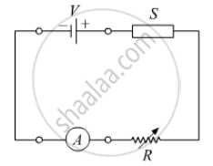
In the following diagram 'S' is a semiconductor. Would you increase or decrease the value of R to keep the reading of the ammeter A constant when S is heated? Give reason for your answer.
Draw a labelled diagram of a full wave rectifier. Show how output voltage varies with time if the input voltage is a sinusoidal voltage.
The graph shown in the figure represents a plot of current versus voltage for a given semiconductor. Identify the region, if any, over which the semiconductor has a negative resistance.

Why is a zener diode considered as a special purpose semiconductor diode?
In a photo diode, the conductive increases when the material is exposed to light. It is found that the conductivity changes only if the wavelength is less than 620 nm. What is the band gap?
(Use Planck constant h = 4.14 × 10⁻¹⁵ eV-s, Boltzmann constant k = 8·62 × 10-5 eV/K.)
The dynamic plate resistance of a triode value is 10 kΩ. Find the change in the plate current if the plate voltage is changed from 200 V to 220 V.
Find the values of rp, µ and gm of a triode operating at plate voltage 200 V and grid voltage −6. The plate characteristics are shown in the figure.

The gain factor of an amplifier in increased from 10 to 12 as the load resistance is changed from 4 kΩ to 8 kΩ. Calculate (a) the amplification factor and (b) the plate resistance.
Diffusion in a p-n junction is due to ______.
With reference to Semiconductor Physics,
Name the diode that emits spontaneous radiation when forward biased.
The current through an ideal PN-junction shown in the following circuit diagram will be:

The nature of binding for a crystal with alternate and evenly spaced positive and negatively ions is
In forward bias width of potential barrier in a p + n junction diode
The expected energy of the electron at absolute zero is called:-
In Figure, Vo is the potential barrier across a p-n junction, when no battery is connected across the junction ______.

If each diode in figure has a forward bias resistance of 25 Ω and infinite resistance in reverse bias, what will be the values of the current I1, I2, I3 and I4?

In the circuit shown in figure, when the input voltage of the base resistance is 10 V, Vbe is zero and Vce is also zero. Find the values of Ib, Ic and β.

Consider a box with three terminals on top of it as shown in figure (a):
 (a) |
Three components namely, two germanium diodes and one resistor are connected across these three terminals in some arrangement. A student performs an experiment in which any two of these three terminals are connected in the circuit shown in figure (b).
 (b) |
The student obtains graphs of current-voltage characteristics for unknown combination of components between the two terminals connected in the circuit. The graphs are
(i) when A is positive and B is negative
 (c) |
(ii) when A is negative and B is positive
 (d) |
(iii) When B is negative and C is positive
|
(e) |

(iv) When B is positive and C is negative
 (f) |
(v) When A is positive and C is negative
 (g) |
(vi) When A is negative and C is positive
 (h) |
From these graphs of current-voltage characteristics shown in figure (c) to (h), determine the arrangement of components between A, B and C.
Draw V-I characteristics of a p-n Junction diode.
Differentiate between the threshold voltage and the breakdown voltage for a diode.
Describe the following term briefly:
Minority carrier injection in forward biasing.
Describe the following term briefly:
Breakdown voltage in reverse biasing
With reference to a semiconductor diode, define the depletion region.
With reference to a semiconductor diode, define the potential barrier.
Choose the correct circuit which can achieve the bridge balance.
