Topics
Electric Charges and Fields
- Electric Charges
- Conductors and Insulators
- Properties of Electric Charge
- Coulomb’s Law
- Forces between Multiple Charges
- Electric Field
- Electric Field Due to a System of Charges
- Physical Significance of Electric Field
- Electric Field Lines
- Electric Flux
- Electric Dipole
- Dipole in a Uniform External Field
- Continuous Charge Distribution
- Gauss’s Law
- Application of Gauss' Law
Electrostatics
Current Electricity
Electrostatic Potential and Capacitance
- Electric Potential and Potential Energy
- Electrostatic Potential
- Electric Potential Due to a Point Charge
- Potential Due to an Electric Dipole
- Potential due to a System of Charges
- Equipotential Surfaces
- Relation Between Electric Field and Electrostatic Potential
- Potential Energy of a System of Charges
- Potential Energy of a Single Charge
- Potential Energy of a System of Two Charges in an External Field
- Potential Energy of a Dipole in an External Field
- Electrostatics of Conductors
- Dielectrics and Polarisation
- Capacitors and Capacitance
- The Parallel Plate Capacitor
- Effect of Dielectric on Capacitance
- Combination of Capacitors
- Energy Stored in a Charged Capacitor
Magnetic Effects of Current and Magnetism
Current Electricity
- Electric Current
- Electric Currents in Conductors
- Ohm's Law
- Drift of Electrons and the Origin of Resistivity
- Mobility of Electrons
- Limitations of Ohm’s Law
- Resistivity of Various Materials
- Temperature Dependence of Resistivity
- Electrical Energy and Power in Conductors
- Cells, EMF, and Internal Resistance
- Cells in Series and in Parallel
- Kirchhoff’s Laws
- Wheatstone Bridge
Moving Charges and Magnetism
- Electromagnetism
- Magnetic force
- Motion in a Magnetic Field
- Magnetic Field Due to a Current-carrying Conductor: Biot-savart's Law
- Applications of Biot-Savart's Law > Magnetic Field at the Axis of a Circular Current-carrying Loop
- Ampere’s Circuital Law
- Solenoid
- Force Between Two Parallel Currents (Ampere’s Law)
- Torque on a Rectangular Current Loop in a Uniform Magnetic Field
- Circular Current Loop as a Magnetic Dipole
- Moving Coil Galvanometer
- Kirchhoff’s Laws
Electromagnetic Induction and Alternating Currents
Electromagnetic Waves
Magnetism and Matter
Optics
Electromagnetic Induction
Alternating Current
Dual Nature of Radiation and Matter
Atoms and Nuclei
Electromagnetic Waves
Electronic Devices
Ray Optics and Optical Instruments
- Ray Optics Or Geometrical Optics
- Reflection of Light by Spherical Mirrors
- Sign Convention for Reflection by Spherical Mirrors
- Focal Length of Spherical Mirrors
- Mirror Equation of Spherical Mirrors
- Refraction of Light
- Total Internal Reflection
- Applications of Total Internal Reflection
- Refraction at a Spherical Surfaces
- Refraction by a Lens
- Power of a Lens
- Combined Focal Length of Two Thin Lenses in Contact
- Refraction of Light through a Prism
- Introduction to Optical Instruments
- Microscope and it’s types
- Telescope
Wave Optics
- Introduction to Wave Optics
- Huygens Principle
- Refraction of a Plane Wave
- Refraction at a Rarer Medium
- Reflection of a Plane Wave by a Plane Surface
- Coherent and Incoherent Addition of Waves
- Interference of Light Waves and Young’s Experiment
- Diffraction of Light
- The Single Slit
- Seeing the Single Slit Diffraction Pattern
- Polarisation of Light
Communication Systems
Dual Nature of Radiation and Matter
- Understanding Dual Nature of Radiation and Matter
- Electron Emission
- Photoelectric Effect - Hertz’s Observations
- Photoelectric Effect - Hallwachs’ and Lenard’s Observations
- Experimental Study of Photoelectric Effect
- Effects of Intensity and Frequency on Photocurrent
- Photoelectric Effect and Wave Theory of Light
- Einstein’s Photoelectric Equation: Energy Quantum of Radiation
- Particle Nature of Light: The Photon
- Wave Nature of Matter
The Special Theory of Relativity
Atoms
Nuclei
Semiconductor Electronics - Materials, Devices and Simple Circuits
Communication Systems
- Detection of Amplitude Modulated Wave
- Production of Amplitude Modulated Wave
- Basic Terminology Used in Electronic Communication Systems
- Sinusoidal Waves
- Modulation and Its Necessity
- Amplitude Modulation (AM)
- Need for Modulation and Demodulation
- Satellite Communication
- Propagation of EM Waves
- Bandwidth of Transmission Medium
- Bandwidth of Signals
The Special Theory of Relativity
- The Special Theory of Relativity
- The Principle of Relativity
- Maxwell'S Laws
- Kinematical Consequences
- Dynamics at Large Velocity
- Energy and Momentum
- The Ultimate Speed
- Twin Paradox
Introduction
Every electronic device — from a simple LED to a smartphone chip — is built from materials chosen for their ability to conduct or resist electricity. Understanding how and why different materials conduct electricity is the foundation of all semiconductor electronics.
Solids are broadly classified based on two key electrical parameters:
| Parameter | Symbol | SI Unit | Relationship |
|---|---|---|---|
| Resistivity | ρ | Ω·m | Lower → better conductor |
| Conductivity | σ | S·m⁻¹ | σ = \[\frac {1}{ρ}\] |
Classification by Resistivity & Conductivity
Comparison Table
| Property | Metals (Conductors) | Semiconductors | Insulators |
|---|---|---|---|
| Resistivity (ρ) | 10−8 to 10−2 Ω·m | 10−5 to 106 Ω·m | 1011 to 1019 Ω·m |
| Conductivity (σ) | 102 to 108 S·m−1 | 10−6 to 105 S·m−1 | 10−19 to 10−11 S·m−1 |
| Band Gap (Eg) | ~0 eV (overlapping bands) | < 3 eV (Si: 1.1 eV, Ge: 0.7 eV) | > 3 eV (Diamond: ~5.4 eV) |
| Effect of Temperature | Resistance increases with temp | Resistance decreases with temp | Remains non-conducting |
| Free electrons at RT | A very large number | Small number (thermally excited) | Virtually none |
| Examples | Cu, Ag, Al, Fe | Si, Ge, GaAs | Glass, Rubber, Diamond |
Energy Band Theory
Formation of Energy Bands
In a single isolated atom, electrons occupy discrete, well-defined energy levels (like rungs of a ladder).
When atoms are packed together in a crystal lattice, electrons are shared among neighbouring atoms. This causes:
- Each discrete energy level splits into closely spaced levels
- These closely spaced levels collectively form an energy band
Analogy: Think of a single tuning fork producing one frequency. When thousands of tuning forks are placed close together, they create a continuous range (band) of frequencies, not a single note.
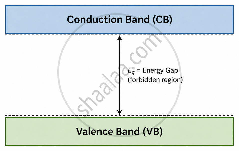
Key Energy Bands
| Band | Description |
|---|---|
| Valence Band (VB) | The highest-energy band that is completely or partially filled with electrons at 0 K. Electrons here are bound to atoms. |
| Forbidden Energy Gap (E_g) | Energy region with no allowed states. Electrons cannot exist here. Also called the Band Gap. |
| Conduction Band (CB) | Energy band above the valence band. Electrons here are free to move and conduct electricity. |
Classification Based on Energy Band Theory
Metals (Conductors)
- Valence band and conduction band overlap (Eg ≈ 0) OR conduction band is partially filled
- A large number of free electrons are available at room temperature (RT)
- Even a tiny applied voltage drives current easily
- Temperature effect: Resistance increases with temperature (increased lattice vibrations scatter electrons)
Insulators
- The valence band is completely filled; the conduction band is completely empty
- Very large energy gap (Eg > 3 eV, e.g., Diamond Eg ≈ 5.4 eV)
- Thermal energy at RT (≈ 0.026 eV) is far too small to excite electrons across the gap
- No conduction possible under normal conditions
Semiconductors
- Valence band completely filled at 0 K → acts as an insulator at absolute zero
- Small energy gap (Eg < 3 eV):
Silicon (Si): Eg = 1.1 eV
Germanium (Ge): Eg = 0.7 eV - At room temperature, some electrons gain sufficient thermal energy to jump into the conduction band, leaving behind holes in the valence band
- Both electrons (in CB) and holes (in VB) contribute to conduction
Types of Semiconductors
Elemental Semiconductors
- Composed of single-element atoms arranged in a crystal lattice
- Each atom has 4 valence electrons, forming covalent bonds with 4 neighbours
- Most important for electronics: Silicon (Si) and Germanium (Ge)
| Property | Silicon (Si) | Germanium (Ge) |
|---|---|---|
| Atomic Number | 14 | 32 |
| Band Gap (E_g) | 1.1 eV | 0.7 eV |
| Melting Point | 1414 °C | 938 °C |
| Common Use | Chips, solar cells | High-speed devices |
Si is preferred over Ge in most devices because its higher band gap provides better stability at room temperature, and its oxide (SiO₂) is an excellent insulator for fabrication.
Compound Semiconductors
Formed by combining two or more elements, it allows tailoring of the band gap for specific applications:
| Category | Examples | Application |
|---|---|---|
| Inorganic | CdS, GaAs, CdSe, InP | LEDs, solar cells, laser diodes |
| Organic | Anthracene, doped phthalocyanines | OLEDs, sensors |
| Organic Polymers | Polypyrrole, polyaniline, polythiophene | Flexible electronics, biosensors |
Real-World Analogy
- A conductor is like a wide-open gateway — electrons flow freely at all times.
- An insulator is like a locked door — no matter how hard you push, nothing gets through.
- A semiconductor is like a turnstile with a spring — it normally stays locked, but with enough push (heat, light, or voltage), it lets electrons through. The more you push, the more it conducts.
