Advertisements
Advertisements
प्रश्न
In a p-n junction, a potential barrier of 250 meV exists across the junction. A hole with a kinetic energy of 300 meV approaches the junction. Find the kinetic energy of the hole when it crosses the junction if the hole approached the junction (a) from the p-side and (b) from the n-side.
Advertisements
उत्तर
Given:
Potential barrier, d = 250 meV
Initially,
Kinetic energy of a hole = 330 meV
We know that the kinetic energy of a hole decreases when the junction is forward biassed (because of the energy loss in crossing the junction).
Also, the kinetic energy of a hole increases when the junction is reverse biassed (because reverse bias voltage pushes the hole on the n-side towards the junction) in the given the p-n junction diode.
(a) The kinetic energy of a hole decreases under forward bias.
∴ Final kinetic energy = (300 − 250) meV
= 50 meV
(b) The kinetic energy of a hole increases under reverse bias.
∴ Final kinetic energy = (300 + 250) meV
= 550 meV
APPEARS IN
संबंधित प्रश्न
A student wants to use two p-n junction diodes to convert alternating current into direct current. Draw the labelled circuit diagram she would use and explain how it works.
Explain, with the help of a circuit diagram, the working of a photo-diode. Write briefly how it is used to detect the optical signals.
If the two ends of a p-n junction are joined by a wire,
A hole diffuses from the p-side to the n-side in a p-n junction. This means that
A semiconducting device is connected in a series circuit with a battery and a resistance. A current is found to pass through the circuit. If the polarity of the battery is reversed, the current drops to almost zero. the device may be
(a) an intrinsic semiconductor
(b) a p-type semiconductor
(c) an n-type semiconductor
(d) a p-n junction
Consider a p-n junction diode having the characteristic \[i - i_0 ( e^{eV/kT} - 1) \text{ where } i_0 = 20\mu A\] . The diode is operated at T = 300 K . (a) Find the current through the diode when a voltage of 300 mV is applied across it in forward bias. (b) At what voltage does the current double?
What are the readings of the ammeters A1 and A2 shown in figure. Neglect the resistance of the meters.
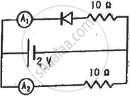
(Assume that the resistance of each diode is zero in forward bias and is infinity in reverse bias.)
Find the current through the battery in each of the circuits shown in figure.
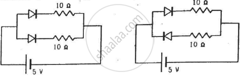
(Assume that the resistance of each diode is zero in forward bias and is infinity in reverse bias.)
Find the current through the resistance R in figure if (a) R = 12Ω (b) R = 48Ω.
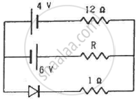
(Assume that the resistance of each diode is zero in forward bias and is infinity in reverse bias.)
Find the equivalent resistance of the network shown in figure between the points A and B.
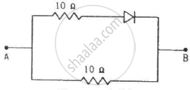
(Assume that the resistance of each diode is zero in forward bias and is infinity in reverse bias.)
An AC source is connected to a diode and a resistor in series. Is the current thorough the resistor AC or DC?
Choose the correct option.
Current through a reverse-biased p-n junction increases abruptly at:
If in a p-n junction diode, a square input signal of 10 V is applied as shown Then the output signal across RL will be ______

In p-n junction diode ______.
What is drift?
What is dynamic resistance?
Why does microscopic roughness prevent a proper crystal lattice from forming between separate p-type and n-type slabs?
How does the interface between physically joined p-type and n-type slabs act on charge carriers?
Which formula gives the static resistance of a diode?
