Advertisements
Advertisements
प्रश्न
A load resistor of 2kΩ is connected in the collector branch of an amplifier circuit using a transistor in common-emitter mode. The current gain β = 50. The input resistance of the transistor is 0.50 kΩ. If the input current is changed by 50µA. (a) by what amount does the output voltage change, (b) by what amount does the input voltage change and (c) what is the power gain?
Advertisements
उत्तर
Given:
Base current gain, \[\beta = 50\]
Change in base current, \[\delta I_b = 50 \mu A\]
Load resistance, \[R_L\] = 2 kΩ
Input resistance, \[R_i\] = 0.50 kΩ
(a) The change in output voltage is given by
\[V_0 = I_c \times R_L \]
\[ \because I_c = \beta \times I_b \]
\[ \therefore V_0 = \beta \times I_b \times R_L \]
\[ \Rightarrow V_0 = 50 \times 50 \mu A \times 2 k\Omega\]
\[ \Rightarrow V_0 = 5 V\]
(b) The change in input voltage is given by
\[\delta V_i = \delta l_b \times R_i \]
\[ \Rightarrow \delta V_i = 50 \times {10}^{- 6} \times 5 \times {10}^2 \]
\[ \Rightarrow \delta V_i = 25 \times {10}^{- 3} \]
\[ \Rightarrow \delta V_i = 25 \text{ mV}\]
(c) Power gain is given by
\[\beta^2 \times \frac{R_L}{R_i}\]
\[ \Rightarrow 2500 \times \frac{2}{0 . 5}\]
\[ \Rightarrow 2500 \times \frac{20}{5} = {10}^4\]
APPEARS IN
संबंधित प्रश्न
In a p-n junction diode, the current I can be expressed as
I = `"I"_0 exp ("eV"/(2"k"_"BT") - 1)`
where I0 is called the reverse saturation current, V is the voltage across the diode and is positive for forward bias and negative for reverse bias, and I is the current through the diode, kBis the Boltzmann constant (8.6×10⁻⁵ eV/K) and T is the absolute temperature. If for a given diode I0 = 5 × 10⁻¹² A and T = 300 K, then
(a) What will be the forward current at a forward voltage of 0.6 V?
(b) What will be the increase in the current if the voltage across the diode is increased to 0.7 V?
(c) What is the dynamic resistance?
(d) What will be the current if reverse bias voltage changes from 1 V to 2 V?
Draw a circuit diagram to study the input and output characteristics of an n-p-n transistor in its common emitter configuration. Draw the typical input and output characteristics.
Consider a p-n junction diode having the characteristic \[i - i_0 ( e^{eV/kT} - 1) \text{ where } i_0 = 20\mu A\] . The diode is operated at T = 300 K . (a) Find the current through the diode when a voltage of 300 mV is applied across it in forward bias. (b) At what voltage does the current double?
Calculate the current through the circuit and the potential difference across the diode shown in figure. The drift current for the diode is 20 µA.
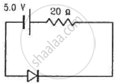
Find the currents through the resistance in the circuits shown in figure.
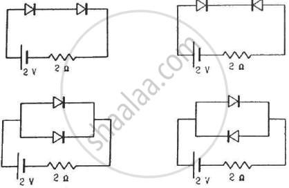
(Assume that the resistance of each diode is zero in forward bias and is infinity in reverse bias.)
Find the current through the battery in each of the circuits shown in figure.
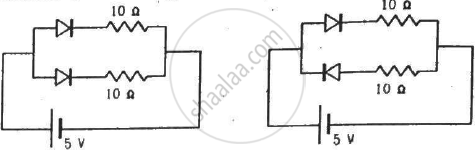
(Assume that the resistance of each diode is zero in forward bias and is infinity in reverse bias.)
When the base current in a transistor is changed from 30µA to 80µA, the collector current is changed from 1.0 mA to 3.5 mA. Find the current gain β.
An AC source is connected to a diode and a resistor in series. Is the current thorough the resistor AC or DC?
In a semiconductor diode, the barrier potential offers opposition to only ______.
p-n junction diode is formed
During the formation of a p-n junction ______.
What is barrier potential?
What is a p-n junction diode?
Which process moves charge carriers from a higher concentration to a lower concentration?
What is drift?
What is static resistance?
How does the interface between physically joined p-type and n-type slabs act on charge carriers?
What role do diodes perform in electronic switching?
In which circuits are diodes used for signal detection?
