Topics
Electrostatics
Electric Charges and Fields
- Electric Charge
- Conductors and Insulators
- Properties of Electric Charge
- Coulomb’s Law
- Forces between Multiple Charges
- Electric Field
- Electric Field Due to a System of Charges
- Physical Significance of Electric Field
- Electric Field Lines
- Electric Flux
- Electric Dipole
- Dipole in a Uniform External Field
- Continuous Charge Distribution
- Gauss’s Law
- Application of Gauss' Law
Current Electricity
Electrostatic Potential and Capacitance
- Electric Potential and Potential Energy
- Electrostatic Potential
- Electric Potential Due to a Point Charge
- Potential Due to an Electric Dipole
- Potential due to a System of Charges
- Equipotential Surfaces
- Relation Between Electric Field and Electrostatic Potential
- Potential Energy of a System of Charges
- Potential Energy of a Single Charge
- Potential Energy of a System of Two Charges in an External Field
- Potential Energy of a Dipole in an External Field
- Electrostatics of Conductors
- Dielectrics and Polarisation
- Capacitors and Capacitance
- The Parallel Plate Capacitor
- Effect of Dielectric on Capacitance
- Combination of Capacitors
- Energy Stored in a Charged Capacitor
Magnetic Effects of Current and Magnetism
Current Electricity
- Electric Current
- Electric Currents in Conductors
- Ohm's Law
- Drift of Electrons and the Origin of Resistivity
- Mobility of Electrons
- Limitations of Ohm’s Law
- Resistivity of Various Materials
- Temperature Dependence of Resistivity
- Electrical Energy and Power in Conductors
- Cells, EMF, and Internal Resistance
- Cells in Series and in Parallel
- Kirchhoff’s Laws
- Wheatstone Bridge
Electromagnetic Induction and Alternating Currents
Moving Charges and Magnetism
- Electromagnetism
- Magnetic force
- Motion in a Magnetic Field
- Magnetic Field Due to a Current-carrying Conductor: Biot-savart's Law
- Applications of Biot-Savart's Law > Magnetic Field at the Axis of a Circular Current-carrying Loop
- Ampere’s Circuital Law
- Solenoid
- Force Between Two Parallel Currents (Ampere’s Law)
- Torque on a Rectangular Current Loop in a Uniform Magnetic Field
- Circular Current Loop as a Magnetic Dipole
- Moving Coil Galvanometer
- Kirchhoff’s Laws
Magnetism and Matter
Electromagnetic Waves
Electromagnetic Induction
Optics
Alternating Current
Dual Nature of Radiation and Matter
Atoms and Nuclei
Electromagnetic Waves
- Introduction to Electromagnetic Waves
- Displacement Current
- Sources of Electromagnetic Waves
- Nature of Electromagnetic Waves
- Electromagnetic Spectrum
- Definition and Characteristics of Electromagnetic Waves
Electronic Devices
Ray Optics and Optical Instruments
- Ray Optics Or Geometrical Optics
- Reflection of Light by Spherical Mirrors
- Sign Convention for Reflection by Spherical Mirrors
- Focal Length of Spherical Mirrors
- Mirror Equation of Spherical Mirrors
- Refraction of Light
- Total Internal Reflection
- Applications of Total Internal Reflection
- Refraction at a Spherical Surfaces
- Refraction by a Lens
- Power of a Lens
- Combined Focal Length of Two Thin Lenses in Contact
- Refraction Through a Prism
- Introduction to Optical Instruments
- Microscope and it’s types
- Telescope
Wave Optics
- Introduction to Wave Optics
- Huygens Principle
- Refraction of a Plane Wave
- Refraction at a Rarer Medium
- Reflection of a Plane Wave by a Plane Surface
- Coherent and Incoherent Addition of Waves
- Interference of Light Waves and Young’s Experiment
- Diffraction of Light
- The Single Slit
- Seeing the Single Slit Diffraction Pattern
- Polarisation of Light
Communication Systems
Dual Nature of Radiation and Matter
- Understanding Dual Nature of Radiation and Matter
- Electron Emission
- Photoelectric Effect - Hertz’s Observations
- Photoelectric Effect - Hallwachs’ and Lenard’s Observations
- Experimental Study of Photoelectric Effect
- Effects of Intensity and Frequency on Photocurrent
- Photoelectric Effect and Wave Theory of Light
- Einstein’s Photoelectric Equation: Energy Quantum of Radiation
- Particle Nature of Light: The Photon
- Wave Nature of Matter
The Special Theory of Relativity
Atoms
Nuclei
Semiconductor Electronics - Materials, Devices and Simple Circuits
Communication Systems
- Detection of Amplitude Modulated Wave
- Production of Amplitude Modulated Wave
- Basic Terminology Used in Electronic Communication Systems
- Sinusoidal Waves
- Modulation and Its Necessity
- Amplitude Modulation (AM)
- Need for Modulation and Demodulation
- Satellite Communication
- Propagation of EM Waves
- Bandwidth of Transmission Medium
- Bandwidth of Signals
The Special Theory of Relativity
- The Special Theory of Relativity
- The Principle of Relativity
- Maxwell'S Laws
- Kinematical Consequences
- Dynamics at Large Velocity
- Energy and Momentum
- The Ultimate Speed
- Twin Paradox
Estimated time: 16 minutes
CBSE: Class 12
Maharashtra State Board: Class 11
Maharashtra State Board: Class 11
Definition: Donor Impurity
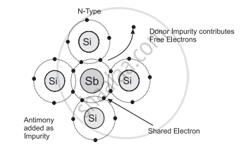
Since every pentavalent dopant atom donates one electron for conduction, it is called a donor impurity.
CBSE: Class 12
Maharashtra State Board: Class 11
Maharashtra State Board: Class 11
N-type Semiconductor
When a silicon or germanium crystal is doped with a pentavalent impurity such as phosphorus, arsenic, or antimony, an n-type semiconductor is obtained.
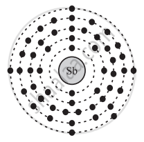
- A dopant atom with 5 valence electrons occupies the position of a silicon atom in the crystal lattice.
- Four electrons from the dopant form bonds with four neighbouring silicon atoms.
- The fifth electron remains very weakly bound to its parent atom.
- Very little energy is needed to free this electron even at room temperature.
- The required energy is 0.01 eV for germanium and 0.05 eV for silicon.
CBSE: Class 12
Maharashtra State Board: Class 11
Maharashtra State Board: Class 11
Origin of the Name N-Type
- In this semiconductor, a large number of electrons are present in the conduction band.
- Its conductivity is due to negatively charged carriers.
- Therefore, it is called an n-type semiconductor.
CBSE: Class 12
Maharashtra State Board: Class 11
Maharashtra State Board: Class 11
Charge Carriers
- The n-type semiconductor also has a few electrons and holes produced due to thermally broken bonds.
- The density of conduction electrons, ne, in a doped semiconductor is the total of electrons contributed by donors and thermally generated electrons from the host.
- The density of holes, nhnh, is only due to the thermal breakdown of some covalent bonds of the host silicon atoms.
- Some electrons and holes recombine continuously because they carry opposite charges.
- The number of free electrons exceeds the number of holes.
- Thus, electrons are the majority carriers, and holes are the minority carriers.
- Relation: ne >> nh
CBSE: Class 12
Maharashtra State Board: Class 11
Maharashtra State Board: Class 11
Energy Band
- The free electrons donated by impurity atoms occupy energy levels in the band gap.
- These levels are close to the conduction band.
- Therefore, these electrons are easily available for conduction.
CBSE: Class 12
Maharashtra State Board: Class 11
Maharashtra State Board: Class 11
Conductivity of Extrinsic Semiconductors
- Extrinsic semiconductors are better conductors than intrinsic semiconductors.
- The conductivity of an extrinsic semiconductor can be controlled by controlling the amount of impurities added.
- The amount of impurities is expressed as parts per million (ppm), that is, one impurity atom per one million atoms of the host.
CBSE: Class 12
Maharashtra State Board: Class 11
Maharashtra State Board: Class 11
Conductivity of Extrinsic Semiconductors
- These are materials doped with pentavalent impurity (donor) atoms.
- Electrical conduction in these materials is due to electrons as the majority charge carriers.
- The donor atom loses electrons and becomes a positively charged ion.
- The number of free electrons is very large compared to the number of holes.
- When energy is supplied externally, negatively charged free electrons (majority charge carriers) and positively charged holes (minority charge carriers) are available for conduction.
CBSE: Class 12
Maharashtra State Board: Class 11
Maharashtra State Board: Class 11
Effect of Doping on Electrical Conductivity
- One cm3 specimen of a metal or semiconductor has of the order of 1022 atoms.
- In a metal, every atom donates at least one free electron for conduction, so 1 cm3 of metal contains of the order of 1022 free electrons.
- 1 cm³ of pure germanium at 20°C contains about 4.2 × 10²² atoms, but only 2.5 × 10¹³ free electrons and 2.5 × 10¹³ holes.
- Addition of 0.001% of arsenic donates 1017 extra free electrons in the same volume.
- The electrical conductivity increases by a factor of 10,000.
Maharashtra State Board: Class 11
Example
Question: A pure silicon crystal has 4 × 1028 atoms m−3. It is doped with a 1 ppm concentration of antimony. Calculate the number of electrons and holes. Given ni = 1.2 × 10¹⁶ m−3.
Given
- Number of silicon atoms = 4 × 1028 m−3
- Doping concentration = 1 ppm = \[\frac {1}{10^6}\]
- ni = 1.2 × 10¹⁶ m−3
Calculation
Number of Sb atoms: \[\frac{4\times10^{28}}{10^6}=4\times10^{22}\]
As one pentavalent impurity atom donates one free electron:
ne = 4 × 10²² m−3
Number of holes: nh = \[\frac {n_i^2}{n_e}\]
\[n_h=\frac{(1.2\times10^{16})^2}{4\times10^{22}}=3.6\times10^9m^{-3}\]
Answer
- Number of free electrons: 4 × 10²² m−3
- Number of holes: 3.6 × 10⁹ m−3
CBSE: Class 12
Maharashtra State Board: Class 11
Maharashtra State Board: Class 11
Key Points: n-type Semiconductor
- An n-type semiconductor is formed by doping silicon or germanium with a pentavalent impurity.
- Pentavalent impurities act as donor impurities.
- The fifth valence electron is weakly bound and can become free easily.
- Electrons are majority carriers and holes are minority carriers.
- For an n-type semiconductor, ne >> nh.
- Donor energy levels lie close to the conduction band.
- Extrinsic semiconductors are better conductors than intrinsic semiconductors.
