Topics
Electrostatics
Electric Charges and Fields
- Electric Charge
- Conductors and Insulators
- Properties of Electric Charge
- Coulomb’s Law
- Forces between Multiple Charges
- Electric Field
- Electric Field Due to a System of Charges
- Physical Significance of Electric Field
- Electric Field Lines
- Electric Flux
- Electric Dipole
- Dipole in a Uniform External Field
- Continuous Charge Distribution
- Gauss’s Law
- Application of Gauss' Law
Current Electricity
Electrostatic Potential and Capacitance
- Electric Potential and Potential Energy
- Electrostatic Potential
- Electric Potential Due to a Point Charge
- Potential Due to an Electric Dipole
- Potential due to a System of Charges
- Equipotential Surfaces
- Relation Between Electric Field and Electrostatic Potential
- Potential Energy of a System of Charges
- Potential Energy of a Single Charge
- Potential Energy of a System of Two Charges in an External Field
- Potential Energy of a Dipole in an External Field
- Electrostatics of Conductors
- Dielectrics and Polarisation
- Capacitors and Capacitance
- The Parallel Plate Capacitor
- Effect of Dielectric on Capacitance
- Combination of Capacitors
- Energy Stored in a Charged Capacitor
Magnetic Effects of Current and Magnetism
Current Electricity
- Electric Current
- Electric Currents in Conductors
- Ohm's Law
- Drift of Electrons and the Origin of Resistivity
- Mobility of Electrons
- Limitations of Ohm’s Law
- Resistivity of Various Materials
- Temperature Dependence of Resistivity
- Electrical Energy and Power in Conductors
- Cells, EMF, and Internal Resistance
- Cells in Series and in Parallel
- Kirchhoff’s Laws
- Wheatstone Bridge
Electromagnetic Induction and Alternating Currents
Moving Charges and Magnetism
- Electromagnetism
- Magnetic force
- Motion in a Magnetic Field
- Magnetic Field Due to a Current-carrying Conductor: Biot-savart's Law
- Applications of Biot-Savart's Law > Magnetic Field at the Axis of a Circular Current-carrying Loop
- Ampere’s Circuital Law
- Solenoid
- Force Between Two Parallel Currents (Ampere’s Law)
- Torque on a Rectangular Current Loop in a Uniform Magnetic Field
- Circular Current Loop as a Magnetic Dipole
- Moving Coil Galvanometer
- Kirchhoff’s Laws
Magnetism and Matter
Electromagnetic Waves
Electromagnetic Induction
Optics
Alternating Current
Dual Nature of Radiation and Matter
Atoms and Nuclei
Electromagnetic Waves
- Introduction to Electromagnetic Waves
- Displacement Current
- Sources of Electromagnetic Waves
- Nature of Electromagnetic Waves
- Electromagnetic Spectrum
- Definition and Characteristics of Electromagnetic Waves
Electronic Devices
Ray Optics and Optical Instruments
- Ray Optics Or Geometrical Optics
- Reflection of Light by Spherical Mirrors
- Sign Convention for Reflection by Spherical Mirrors
- Focal Length of Spherical Mirrors
- Mirror Equation of Spherical Mirrors
- Refraction of Light
- Total Internal Reflection
- Applications of Total Internal Reflection
- Refraction at a Spherical Surfaces
- Refraction by a Lens
- Power of a Lens
- Combined Focal Length of Two Thin Lenses in Contact
- Refraction Through a Prism
- Introduction to Optical Instruments
- Microscope and it’s types
- Telescope
Wave Optics
- Introduction to Wave Optics
- Huygens Principle
- Refraction of a Plane Wave
- Refraction at a Rarer Medium
- Reflection of a Plane Wave by a Plane Surface
- Coherent and Incoherent Addition of Waves
- Interference of Light Waves and Young’s Experiment
- Diffraction of Light
- The Single Slit
- Seeing the Single Slit Diffraction Pattern
- Polarisation of Light
Communication Systems
Dual Nature of Radiation and Matter
- Understanding Dual Nature of Radiation and Matter
- Electron Emission
- Photoelectric Effect - Hertz’s Observations
- Photoelectric Effect - Hallwachs’ and Lenard’s Observations
- Experimental Study of Photoelectric Effect
- Effects of Intensity and Frequency on Photocurrent
- Photoelectric Effect and Wave Theory of Light
- Einstein’s Photoelectric Equation: Energy Quantum of Radiation
- Particle Nature of Light: The Photon
- Wave Nature of Matter
The Special Theory of Relativity
Atoms
Nuclei
Semiconductor Electronics - Materials, Devices and Simple Circuits
Communication Systems
- Detection of Amplitude Modulated Wave
- Production of Amplitude Modulated Wave
- Basic Terminology Used in Electronic Communication Systems
- Sinusoidal Waves
- Modulation and Its Necessity
- Amplitude Modulation (AM)
- Need for Modulation and Demodulation
- Satellite Communication
- Propagation of EM Waves
- Bandwidth of Transmission Medium
- Bandwidth of Signals
The Special Theory of Relativity
- The Special Theory of Relativity
- The Principle of Relativity
- Maxwell'S Laws
- Kinematical Consequences
- Dynamics at Large Velocity
- Energy and Momentum
- The Ultimate Speed
- Twin Paradox
Maharashtra State Board: Class 11
Definition: p-type Semiconductor
A p-type semiconductor is a semiconductor obtained by doping pure silicon or germanium with a trivalent impurity so that holes become the majority charge carriers.
Maharashtra State Board: Class 11
Formula: p-type semiconductor
If hole concentration is high, then:
This is especially important for numerical problems in board examinations and entrance tests.
Maharashtra State Board: Class 11
Formation of p-type Semiconductor
Pure silicon and germanium are tetravalent elements, which means each atom forms four covalent bonds. When a trivalent impurity atom such as boron is added, it can form only three covalent bonds, leaving one bond incomplete. This incomplete bond appears as a hole.
Dopants Used
- Boron (B)
- Aluminium (Al)
- Indium (In)
During doping:
- A trivalent impurity replaces a silicon or germanium atom in the crystal lattice.
- Only three covalent bonds are completed.
- One bond remains deficient by one electron.
- This deficiency behaves like a hole.
- As a result, the semiconductor becomes p-type.
Maharashtra State Board: Class 11
Generation of Holes
The trivalent impurity has only three valence electrons, but the lattice requires four electrons for bonding. Therefore, a vacancy is created in one covalent bond. This vacancy can accept an electron from a neighbouring bond and is therefore associated with an acceptor impurity.
- Trivalent impurities in p-type semiconductors are called acceptor impurities because they accept an electron.
- The missing electron position is called a hole.
Maharashtra State Board: Class 11
Majority and Minority Carriers
In a p-type semiconductor, holes are present in very large numbers because of doping, while a small number of electrons still exist due to thermal generation. Therefore, holes are the majority carriers and electrons are the minority carriers.
| Charge carrier | Role in a p-type semiconductor |
|---|---|
| Holes | Majority carriers |
| Electrons | Minority carriers |
Very Important Relation
For a p-type semiconductor:
- nh ≫ ne
- nenh = \[n_i^2\]
Where:
- nh = hole concentration
- ne = electron concentration
- ni = intrinsic carrier concentration
Energy Band
The energy band description of a p-type semiconductor shows that the trivalent impurity introduces an acceptor energy level slightly above the valence band. Because this level is close to the valence band, electrons can easily move from the valence band to the acceptor level, leaving behind holes in the valence band.
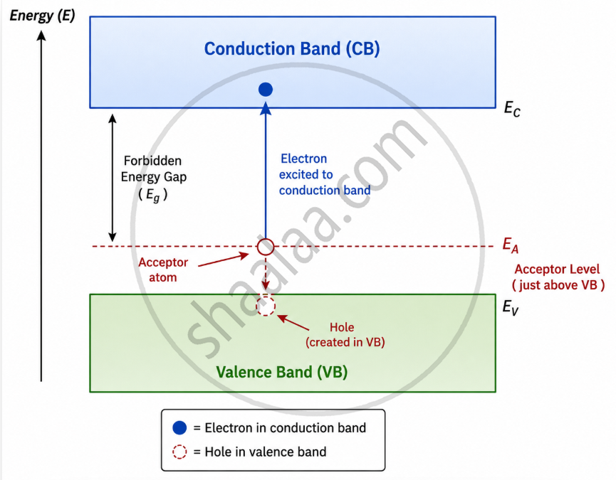
Band Interpretation
- The valence band contains a large number of holes after doping.
- The acceptor level lies just above the valence band.
- Electrons require only a small amount of energy to shift to the acceptor level.
- Hole conduction becomes dominant.
Maharashtra State Board: Class 11
Conduction in a P-Type Semiconductor
Although holes appear to move, the actual particles that move are electrons. When one electron fills a hole, it leaves another hole behind. In this way, the hole appears to move through the crystal.
Stepwise explanation
- A neighbouring electron jumps into a hole.
- A new hole is created where that electron came from.
- Repetition of this process makes the hole appear to move.
- Thus, the current in a p-type semiconductor is mainly due to hole motion.
Analogy
Think of a row of seats with one empty seat. When one person shifts into the empty seat, a new empty seat appears at the old position. The empty seat seems to move, although only people actually move. In the same way, holes appear to move, though electrons are the real moving particles.
Maharashtra State Board: Class 11
Main characteristics of p-type semiconductor
- Formed by doping pure silicon or germanium with a trivalent impurity.
- Holes are the majority carriers.
- Electrons are the minority carriers.
- The crystal remains electrically neutral as a whole.
- The acceptor level lies close to the valence band.
- Conductivity increases relative to that of the intrinsic semiconductor.
Maharashtra State Board: Class 11
p-type vs n-type Semiconductor
| Feature | p-type semiconductor | n-type semiconductor |
|---|---|---|
| Dopant used | Trivalent impurity | Pentavalent impurity |
| Examples of dopant | B, Al, In | P, As, Sb |
| Majority carriers | Holes | Electrons |
| Minority carriers | Electrons | Holes |
| Impurity type | Acceptor | Donor |
| Energy level introduced | Near the valence band | Near the conduction band |
Example 1
Given:
- ni = 1.5 × 10¹⁶ m−3
- nh = 4.5 × 10²² m−3
Solution:
- Use the mass action law: nenh = \[n_i^2\]
- Rearrange to find electron concentration: ne = \[\frac {n_i^2}{n_h}\]
- Substitute the given values: ne = \[\frac{(1.5\times10^{16})^2}{4.5\times10^{22}}\]
- Calculate: ne = 5 × 10⁹ m−3
Answer: ne = 5 × 10⁹ m−3
Example 2
Given:
- Number of Si atoms = 5 × 1028 m−3
- Doping concentration = 1 ppm
- ni = 1.5 × 10¹⁶ m−3
Solution:
- Calculate donor concentration:ND = 5 × 1028 × 10−6 = 5 × 10²² m−3
- Since the semiconductor is heavily doped, ne ≈ ND = 5 × 10²² m−3
- Use the mass action law: nenh = \[n_i^2}\]
- Calculate hole concentration:
nh = \[\frac{(1.5\times10^{16})^2}{5\times10^{22}}=4.5\times10^9\mathrm{~m}^{-3}\]
Answer: ne = 5 × 10²² m−3, nh = 4.5 × 10⁹ m−3
