Advertisements
Advertisements
Question
Explain the working of P-N junction diode in forward and reverse biased mode.
Advertisements
Solution
If a germanium crystal or silicon crystal is doped during manufacture in such a way that half of it is p-type and other half is n-type, we get p-n junction.
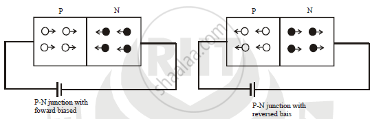
(a) Forward biased: A battery is connected across p-n junction diode such that, p-type is connected to positive terminal and n-type is connected to negative terminal, then it is called forward biased. The potential difference applied should be more than 0.3 V for germanium and more than 0.7 V for silicon. Then holes from p-type region and electrons from n-type region moves towards barrier and it decreases width and height of
barrier. Hence an electric current flows through circuit. When applied potential is zero, then current also equal to zero. When P.D. Increases the current is also increases but very slowly. When applied P.D. is more than potential barrier, current in creases rapidly. This voltage is called knee voltage. The forward biased voltage at which the current through diode increases rapidly is called knee voltage
b) Reversed biased : A battery is connected across p-n junction diode such that, p-type is connected to negative terminal and n-type is connected to positive terminal, then it is called reversed biased. The holes from p type region and electrons from n-type region moves away from junction and it increases width and height of barrier. Hence there is no flow of an electric current in ideal case. In actual case current is very small (inμA) . The width of potential barrier increases and diode offer very high resistance. The very small current flows through circuit is called as reverse current. If reversed bias voltage increased then the kinetic energy of electrons increases. At certain reversed bias voltage the K.E. of electrons increases enough and they knock out the electrons from semiconductor atoms\ Therefore current suddenly increase. That certain reversed bias voltage is called as breakdown voltage. At breakdown voltage the current increases suddenly and destroy the junction permanently. The reversed bas voltage at which P-N junction breaks and current suddenly increases is called as breakdown voltage.
APPEARS IN
RELATED QUESTIONS
With reference to semiconductor devices, define a p-type semiconductor and a Zener diode.
What is the use of Zener diode?
Plot a graph showing variation of current versus voltage for the material GaAs ?
The power delivered in the plate circular of a diode is 1.0 W when the plate voltage is 36 V. Find the power delivered if the plate voltage is increased to 49 V. Assume Langmuir-Child equation to hold.
A triode value operates at Vp = 225 V and Vg = −0.5 V.
The plate current remains unchanged if the plate voltage is increased to 250 V and the grid voltage is decreased to −2.5 V. Calculate the amplification factor.
The gain factor of an amplifier in increased from 10 to 12 as the load resistance is changed from 4 kΩ to 8 kΩ. Calculate (a) the amplification factor and (b) the plate resistance.
With reference to a semiconductor diode, what is meant by:
(i) Forward bias
(ii) Reverse bias
(iii) Depletion region
Answer the following question.
Why photodiodes are required to operate in reverse bias? Explain.
What are the applications of p - n Junction diode?
Of the diodes shown in the following diagrams, which one is reverse biased?
A – pn junction has a depletion layer of thickness .of the order of
When we apply reverse biased to a junction diode, it
The nature of binding for a crystal with alternate and evenly spaced positive and negatively ions is
In forward bias width of potential barrier in a p + n junction diode
In the depletion region of a diode ______.
- there are no mobile charges.
- equal number of holes and electrons exist, making the region neutral.
- recombination of holes and electrons has taken place.
- immobile charged ions exist.
The breakdown in a reverse biased p–n junction diode is more likely to occur due to ______.
- large velocity of the minority charge carriers if the doping concentration is small.
- large velocity of the minority charge carriers if the doping concentration is large.
- strong electric field in a depletion region if the doping concentration is small.
- strong electric field in the depletion region if the doping concentration is large.
Can the potential barrier across a p-n junction be measured by simply connecting a voltmeter across the junction?
If each diode in figure has a forward bias resistance of 25 Ω and infinite resistance in reverse bias, what will be the values of the current I1, I2, I3 and I4?

The graph of potential barrier versus width of depletion region for an unbiased diode is shown in graph A. In comparison to A, graphs B and C are obtained after biasing the diode in different ways. Identify the type of biasing in B and C and justify your answer
| ‘A’ | ‘B’ | ‘C’ |
 |
 |
 |
Write the property of a junction diode which makes it suitable for rectification of ac voltages.
Explain the formation of the barrier potential in a p-n junction.
Answer the following giving reasons:
A p-n junction diode is damaged by a strong current.
A semiconductor device is connected in series with a battery, an ammeter and a resistor. A current flows in the circuit. If. the polarity of the battery is reversed, the current in the circuit almost becomes zero. The device is a/an ______.
An ideal PN junction diode offers ______.
Choose the correct circuit which can achieve the bridge balance.
