Advertisements
Advertisements
The drift current in a p-n junction is 20.0 µA. Estimate the number of electrons crossing a cross section per second in the depletion region.
Concept: undefined >> undefined
The current−voltage characteristic of an ideal p-n junction diode is given by \[i = i_0 ( e^{eV/KT} - 1)\] where, the drift current i0 equals 10 µA. Take the temperature T to be 300 K. (a) Find the voltage V0 for which \[e^{eV/kT} = 100 .\]One can neglect the term 1 for voltages greater than this value. (b) Find an expression for the dynamic resistance of the diode as a function of V for V > V0. (c) Find the voltage for which the dynamic resistance is 0.2 Ω.
(Use Planck constant h = 4.14 × 10⁻¹⁵ eV-s, Boltzmann constant k = 8·62 × 10-5 eV/K.)
Concept: undefined >> undefined
Advertisements
Consider a p-n junction diode having the characteristic \[i - i_0 ( e^{eV/kT} - 1) \text{ where } i_0 = 20\mu A\] . The diode is operated at T = 300 K . (a) Find the current through the diode when a voltage of 300 mV is applied across it in forward bias. (b) At what voltage does the current double?
Concept: undefined >> undefined
Calculate the current through the circuit and the potential difference across the diode shown in figure. The drift current for the diode is 20 µA.

Concept: undefined >> undefined
Each of the resistance shown in figure has a value of 20 Ω. Find the equivalent resistance between A and B. Does it depend on whether the point A or B is at higher potential?

Concept: undefined >> undefined
Find the currents through the resistance in the circuits shown in figure.

(Assume that the resistance of each diode is zero in forward bias and is infinity in reverse bias.)
Concept: undefined >> undefined
What are the readings of the ammeters A1 and A2 shown in figure. Neglect the resistance of the meters.

(Assume that the resistance of each diode is zero in forward bias and is infinity in reverse bias.)
Concept: undefined >> undefined
Find the current through the battery in each of the circuits shown in figure.

(Assume that the resistance of each diode is zero in forward bias and is infinity in reverse bias.)
Concept: undefined >> undefined
Find the current through the resistance R in figure if (a) R = 12Ω (b) R = 48Ω.

(Assume that the resistance of each diode is zero in forward bias and is infinity in reverse bias.)
Concept: undefined >> undefined
Draw the current-voltage characteristics for the device show in figure between the terminals A and B.

(Assume that the resistance of each diode is zero in forward bias and is infinity in reverse bias.)
Concept: undefined >> undefined
Find the equivalent resistance of the network shown in figure between the points A and B.

(Assume that the resistance of each diode is zero in forward bias and is infinity in reverse bias.)
Concept: undefined >> undefined
When the base current in a transistor is changed from 30µA to 80µA, the collector current is changed from 1.0 mA to 3.5 mA. Find the current gain β.
Concept: undefined >> undefined
A load resistor of 2kΩ is connected in the collector branch of an amplifier circuit using a transistor in common-emitter mode. The current gain β = 50. The input resistance of the transistor is 0.50 kΩ. If the input current is changed by 50µA. (a) by what amount does the output voltage change, (b) by what amount does the input voltage change and (c) what is the power gain?
Concept: undefined >> undefined
As the speed of a particle increases, its rest mass _______________ .
Concept: undefined >> undefined
An AC source is connected to a diode and a resistor in series. Is the current thorough the resistor AC or DC?
Concept: undefined >> undefined
A diode, a resistor and a 50 Hz AC source are connected in series. The number of current pulses per second through the resistor is __________ .
Concept: undefined >> undefined
In the following diagram 'S' is a semiconductor. Would you increase or decrease the value of R to keep the reading of the ammeter A constant when S is heated? Give reason for your answer.
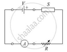
Concept: undefined >> undefined
Draw its I – V characteristics of photodiode
Concept: undefined >> undefined
Find the wavelength of the electron orbiting in the first excited state in hydrogen atom.
Concept: undefined >> undefined
In the following diagram, is the junction diode forward biased or reverse biased ?
Concept: undefined >> undefined
