Advertisements
Advertisements
Plot a graph showing variation of current versus voltage for the material GaAs ?
Concept: Semiconductor Diode
Draw a circuit diagram to study the input and output characteristics of an n-p-n transistor in its common emitter configuration. Draw the typical input and output characteristics.
Concept: Diode or p-n Junction
Explain, with the help of a circuit diagram, the working of n-p-n transistor as a common emitter amplifier.
Concept: Diode or p-n Junction
How is a zener diode fabricated so as to make it a special purpose diode? Draw I-V characteristics of zener diode and explain the significance of breakdown voltage.
Explain briefly, with the help of a circuit diagram, how a p-n junction diode works as a half wave rectifier.
Concept: Diode or p-n Junction
In a pure semiconductor crystal of Si, if antimony is added then what type of extrinsic semiconductor is obtained. Draw the energy band diagram of this extrinsic semiconductor so formed.
Concept: Extrinsic Semiconductor
ASSERTION (A): The electrical conductivity of a semiconductor increases on doping.
REASON (R): Doping always increases the number of electrons in the semiconductor.
Concept: Classification of Metals, Conductors and Semiconductors
The figure shows a piece of pure semiconductor S in series with a variable resistor R and a source of constant voltage V. Should the value of R be increased or decreased to keep the reading of the ammeter constant, when semiconductor S is heated? Justify your answer

Concept: Extrinsic Semiconductor
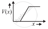
The graph of potential barrier versus width of depletion region for an unbiased diode is shown in graph A. In comparison to A, graphs B and C are obtained after biasing the diode in different ways. Identify the type of biasing in B and C and justify your answer
| ‘A’ | ‘B’ | ‘C’ |
 |
 |
 |
Concept: Semiconductor Diode
Draw V-I characteristics of a p-n Junction diode.
Concept: Semiconductor Diode
Differentiate between the threshold voltage and the breakdown voltage for a diode.
Concept: Semiconductor Diode
Two crystals C1 and C2, made of pure silicon, are doped with arsenic and aluminium respectively.
Identify the extrinsic semiconductors so formed.
Concept: Extrinsic Semiconductor
Two crystals C1 and C2, made of pure silicon, are doped with arsenic and aluminium respectively.
Why is doping of intrinsic semiconductors necessary?
Concept: Intrinsic Semiconductor
Name the extrinsic semiconductors formed when pure germanium is doped with a trivalent impurity. Draw the energy band diagram of extrinsic semiconductors so formed.
Concept: Extrinsic Semiconductor
Name the extrinsic semiconductors formed when pure germanium is doped with a Pentavalent impurity. Draw the energy band diagram of extrinsic semiconductors so formed.
Concept: Extrinsic Semiconductor
A semiconductor device is connected in series with a battery, an ammeter and a resistor. A current flows in the circuit. If. the polarity of the battery is reversed, the current in the circuit almost becomes zero. The device is a/an ______.
Concept: Semiconductor Diode
- Assertion (A): The resistance of an intrinsic semiconductor decreases with an increase in its temperature.
- Reason (R): The number of conduction electrons as well as hole increase in an intrinsic semiconductor with the rise in its temperature.
Concept: Intrinsic Semiconductor
- Assertion (A): Putting the p-type semiconductor slab directly in physical contact with the n-type semiconductor slab cannot form the pn junction.
- Reason (R): The roughness at contact will be much more than inter atomic crystal spacing and continuous flow of charge carriers is not possible.
Concept: Extrinsic Semiconductor
Read the following paragraph and answer the questions that follow.
| A semiconductor diode is basically a pn junction with metallic contacts provided at the ends for the application of an external voltage. It is a two-terminal device. When an external voltage is applied across a semiconductor diode such that the p-side is connected to the positive terminal of the battery and the n-side to the negative terminal, it is said to be forward-biased. When an external voltage is applied across the diode such that the n-side is positive and the p-side is negative, it is said to be reverse-biased. An ideal diode is one whose resistance in forward biasing is zero and the resistance is infinite in reverse biasing. When the diode is forward biased, it is found that beyond forward voltage called knee voltage, the conductivity is very high. When the biasing voltage is more than the knee voltage the potential barrier is overcome and the current increases rapidly with an increase in forward voltage. When the diode is reverse biased, the reverse bias voltage produces a very small current of about a few microamperes which almost remains constant with bias. This small current is a reverse saturation current. |
- In the given figure, a diode D is connected to an external resistance R = 100 Ω and an emf of 3.5 V. If the barrier potential developed across the diode is 0.5 V, the current in the circuit will be:
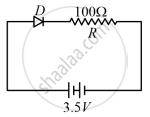
(a) 40 mA
(b) 20 mA
(c) 35 mA
(d) 30 mA - In which of the following figures, the pn diode is reverse biased?
(a)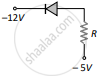
(b)
(c)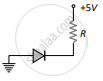
(d)
- Based on the V-I characteristics of the diode, we can classify the diode as:
(a) bilateral device
(b) ohmic device
(c) non-ohmic device
(d) passive element
OR
Two identical PN junctions can be connected in series by three different methods as shown in the figure. If the potential difference in the junctions is the same, then the correct connections will be:
(a) in the circuits (1) and (2)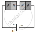

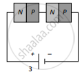
(b) in the circuits (2) and (3)
(c) in the circuits (1) and (3)
(d) only in the circuit (1) 
The V-I characteristic of a diode is shown in the figure. The ratio of the resistance of the diode at I = 15 mA to the resistance at V = -10 V is
(a) 100
(b) 106
(c) 10
(d) 10-6
Concept: Semiconductor Diode
A signal of 5 kHz frequency is amplitude modulated on a carrier wave of frequency 2 MHz. What are the frequencies of the side bands produced?
Concept: Amplitude Modulation (AM)
Why is base band signal not transmitted directly? Give any two reasons
Concept: Need for Modulation and Demodulation
