Advertisements
Advertisements
Draw a circuit diagram of an n-p-n transistor with its emitter-base junction forward biased and basecollector junction reverse biased. Briefly describe its working.
Explain how a transistor in its active state exhibits a low resistance at its emitter-base junction and high resistance at its base-collector junction.
Concept: Junction Transistor >> Basic Transistor Circuit Configurations and Transistor Characteristics
Derive the expression for the voltage gain of a transistor amplifier in CE configuration in terms of the load resistance RL, current gain a βa and input resistance.
Explain why input and output voltages are in opposite phase.
Concept: Junction Transistor >> Basic Transistor Circuit Configurations and Transistor Characteristics
Write the important considerations which are to be taken into account while fabricating a p-n junction diode to be used as a Light Emitting Diode (LED). What should be the order of band gap of an LED, if it is required to emit light in the visible range? Draw a circuit diagram and explain its action.
Concept: Special Purpose P-n Junction Diodes
Draw the circuit arrangement for studying the output characteristics of n-p-n transistor in CE configuration. Explain how the output characteristics are obtained.
Concept: Transistor Action
Draw a circuit diagram of an n-p-n transistor with its emitter-base junction forward biased and base-collector junction reverse biased. Briefly describe its working.
Explain how a transistor in its active state exhibits a low resistance at its emitter-base junction and high resistance at its base-collector junction.
Concept: Junction Transistor >> Basic Transistor Circuit Configurations and Transistor Characteristics
Derive the expression for the voltage gain of a transistor amplifier in CE configuration in terms of the load resistance RL, current gain βa and input resistance.
Explain why input and output voltages are in the opposite phase.
Concept: Junction Transistor >> Basic Transistor Circuit Configurations and Transistor Characteristics
Write the important considerations which are to be taken into account while fabricating a p-n junction diode to be used as a Light Emitting Diode (LED). What should be the order of the band gap of an LED, if it is required to emit light in the visible range? Draw a circuit diagram and explain its action.
Concept: Special Purpose P-n Junction Diodes
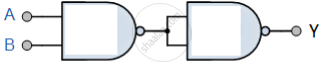
The outputs of two NOT gates are fed to a NOR gate. Draw the logic circuit of the combination of gates. Write its truth table. Identify the gate equivalent to this circuit.
Concept: Digital Electronics and Logic Gates
You are given circuit as shown in the figure, which consists of NAND gate. Identify the logic operation carried out by the two. Write the truth table. Identify the gates equivalent to the tow circuits.
Concept: Digital Electronics and Logic Gates
Answer the following question.
Draw the circuit arrangement for studying the output characteristics of an n-p-n transistor in CE configuration. Explain how the output characteristics is obtained.
Concept: Junction Transistor >> Basic Transistor Circuit Configurations and Transistor Characteristics
What is a solar cell?
Concept: Special Purpose P-n Junction Diodes
You are given a circuit as shown in the figure, which consists of the NAND gate. Identify the logic operation carried out by the two. Write the truth table. Identify the gates equivalent to the tow circuit.
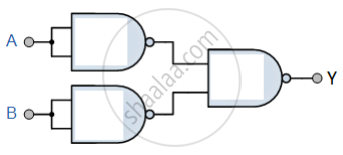
Concept: Digital Electronics and Logic Gates
In a pure semiconductor crystal of Si, if antimony is added then what type of extrinsic semiconductor is obtained. Draw the energy band diagram of this extrinsic semiconductor so formed.
Concept: Extrinsic Semiconductor
Name the device which converts the change in intensity of illumination to change in electric current flowing through it. Plot I-V characteristics of this device for different intensities. State any two applications of this device.
Concept: Special Purpose P-n Junction Diodes
Explain with a proper diagram how an ac signal can be converted into dc (pulsating) signal with output frequency as double than the input frequency using pn junction diode. Give its input and output waveforms.
Concept: Application of Junction Diode as a Rectifier
ASSERTION (A): The electrical conductivity of a semiconductor increases on doping.
REASON (R): Doping always increases the number of electrons in the semiconductor.
Concept: Classification of Metals, Conductors and Semiconductors
The figure shows a piece of pure semiconductor S in series with a variable resistor R and a source of constant voltage V. Should the value of R be increased or decreased to keep the reading of the ammeter constant, when semiconductor S is heated? Justify your answer

Concept: Extrinsic Semiconductor
The graph of potential barrier versus width of depletion region for an unbiased diode is shown in graph A. In comparison to A, graphs B and C are obtained after biasing the diode in different ways. Identify the type of biasing in B and C and justify your answer
| ‘A’ | ‘B’ | ‘C’ |
 |
 |
 |
Concept: Semiconductor Diode
Read the following paragraph and answer the questions.
|
LED is a heavily doped P-N junction which under forward bias emits spontaneous radiation. When it is forward-biased, due to recombination of holes and electrons at the junction, energy is released in the form of photons. In the case of Si and Ge diode, the energy released in recombination lies in the infrared region. LEDs that can emit red, yellow, orange, green and blue light are commercially available. The semiconductor used for fabrication of visible LEDs must at least have a band gap of 1.8 eV. The compound semiconductor Gallium Arsenide – Phosphide is used for making LEDs of different colours.
|

- Why are LEDs made of compound semiconductor and not of elemental semiconductors?
- What should be the order of bandgap of an LED, if it is required to emit light in the visible range?
- A student connects the blue coloured LED as shown in the figure. The LED did not glow when switch S is closed. Explain why?

OR
iii. Draw V-I characteristic of a p-n junction diode in
(i) forward bias and (ii) reverse bias
Concept: Special Purpose P-n Junction Diodes
With the help of a circuit diagram, explain briefly how a p-n junction diode works as a half-wave rectifier.
Concept: Application of Junction Diode as a Rectifier
