Advertisements
Advertisements
Question
Derive the expression for the voltage gain of a transistor amplifier in CE configuration in terms of the load resistance RL, current gain βa and input resistance.
Explain why input and output voltages are in the opposite phase.
Advertisements
Solution
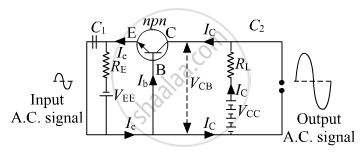
Let Ri be the input resistance of the emitter-base circuit. When an input signal voltage Vi is applied to the emitter-base circuit, let ΔIb, ΔIc be the change in base current and collector current respectively.
Then, Vi = ΔIb × Ri
Then ac current gain of the transistor is,
Current gain, `beta_"a" = (Delta "I"_"C")/(Delta "I"_"B")`
⇒ Δ IC = βa × ΔIB
Also, VCE = VCC -ICRL
As the change in the base current changes the collector current but not VCC, so,
ΔVCE = 0 - ΔICR = - (βa Δ IB) RL
Output voltage, V0 = ΔVCE - βa Δ IBRL
The voltage gain of the common emitter amplifier,
`"AV" = "V"_0/"V"_"i" = (-beta Delta "I"_"B""R"_"L")/(Delta "I"_"B""R"_"i") = -beta_"a" "R"_"L"/("R"_"i")`
`"AV" -beta_"a" "R"_"L"/("R"_"i")`
Here, -ve sign shows that the output voltage is 180o out of phase with the input voltage. i.e. input voltage and output voltage are in the opposite phase. As the input voltage rises, so the current increases through the base circuit, this increases the current through the collector circuit. This results in the voltage between the collector and emitter terminals falling.
