Advertisements
Advertisements
Question
Draw a circuit diagram of an n-p-n transistor with its emitter-base junction forward biased and base-collector junction reverse biased. Briefly describe its working.
Explain how a transistor in its active state exhibits a low resistance at its emitter-base junction and high resistance at its base-collector junction.
Advertisements
Solution
an n-p-n transistor with an emitter-base junction is forward biased and base-collector junction reverses biased:
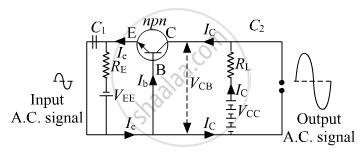
Working: The figure shows the emitter-base junction is forward biased and the collector-base junction is reversed biased. When the input signal voltage is fed to the emitter-base current, it changes the emitter-base voltage and hence the emitter current. Which in turn changes the collector current. Due to it, the collector voltage VCB varies in accordance with the relation VCB =VCC - ICRL. This variation in collector voltage appears as an amplified output(Vo)
For an n-p-n transistor in the active state, resistance is kept low at the emitter-base junction and high at the base-collector junction because the n-p-n transistor is used to amplify the low voltage input to a high voltage out. As the input is applied at the emitter-base junction hence for a low input voltage the resistance at the emitter-base junction is kept low, and the output is obtained at base-collector, so for high voltage output, resistance is kept low at the base-collector junction.
