Advertisements
Advertisements
Question
Read the following paragraph and answer the questions.
|
LED is a heavily doped P-N junction which under forward bias emits spontaneous radiation. When it is forward-biased, due to recombination of holes and electrons at the junction, energy is released in the form of photons. In the case of Si and Ge diode, the energy released in recombination lies in the infrared region. LEDs that can emit red, yellow, orange, green and blue light are commercially available. The semiconductor used for fabrication of visible LEDs must at least have a band gap of 1.8 eV. The compound semiconductor Gallium Arsenide – Phosphide is used for making LEDs of different colours.
|
- Why are LEDs made of compound semiconductor and not of elemental semiconductors?
- What should be the order of bandgap of an LED, if it is required to emit light in the visible range?
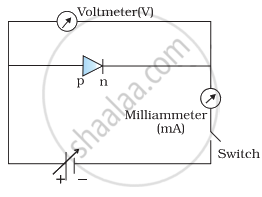
- A student connects the blue coloured LED as shown in the figure. The LED did not glow when switch S is closed. Explain why?

OR
iii. Draw V-I characteristic of a p-n junction diode in
(i) forward bias and (ii) reverse bias
Advertisements
Solution
- LEDs are made up of compound semiconductors and not by the elemental conductor because the band gap in the elemental conductor has a value that can detect the light of a wavelength which lies in the infrared (IR) region.
- 1.8 eV to 3 eV
- LED is reversed-biased that is why it is not glowing.
OR
iii. (i) forward bias -

(ii) reverse bias

APPEARS IN
RELATED QUESTIONS
Colour of light emitted by LED depends upon__________________ .
- its forward bias
- its reverse bias
- the band gap of the material of semiconductor
- its size
Explain with the help of a diagram, how depletion region and potential barrier are formed in a junction diode.
Carbon, silicon and germanium have four valence electrons each. These are characterised by valence and conduction bands separated by energy band gap respectively equal to (Eg)C, (Eg)Si and (Eg)Ge. Which of the following statements is true?
Draw the circuit diagram of a full wave rectifier using p-n junction diode.
Explain its working and show the output, input waveforms.
The plate resistance of a triode is 8 kΩ and the transconductance is 2.5 millimho. (a) If the plate voltage is increased by 48 V and the grid voltage is kept constant, what will be the increase in the plate current? (b) With plate voltage kept constant at this increased value, by how much should the grid voltage be decreased in order to bring the plate current back to its initial value?
Write the important considerations which are to be taken into account while fabricating a p-n junction diode to be used as a Light Emitting Diode (LED). What should be the order of band gap of an LED, if it is required to emit light in the visible range? Draw a circuit diagram and explain its action.
Explain the three processes involved in the working of a solar cell.
With reference to Semiconductor Physics,
Name the process that causes depletion region in a p-n junction.
Briefly explain how emf is generated in a solar cell.
Identify the special purpose diodes 'A', 'B' and 'C' from the given symbols.


