English

Draw the Circuit Diagram of a Full Wave Rectifier Using P-n Junction Diode. Explain Its Working and Show the Output, Input Waveforms. - Physics

Advertisements
Advertisements

Question

Draw the circuit diagram of a full wave rectifier using p-n junction diode.

Explain its working and show the output, input waveforms.

Advertisements

Solution

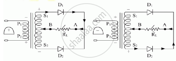
Full wave rectifier:

When the diode rectifies the whole of the AC wave, it is called full wave rectifier.

The figure shows the arrangement for using diode as full wave rectifier. The alternating input signal is fed to the primary P1P2 of a transformer. The output signal appears across the load resistance RL.

During the positive half of the input signal, suppose P1 and P2 are negative and positive respectively. This would mean that S1 and S2 are positive and negative respectively. Therefore, the diode D1 is forward biased and D2 is reverse biased. The flow of current in the load resistance RL is from A to B.

During the negative half of the input signal, S1 and S2 are negative and positive respectively. Therefore, the diode D1 is reverse biased and D2 is forward biased. The flow of current in the load resistance RL is from A to B.

shaalaa.com
  Is there an error in this question or solution?
2011-2012 (March) Delhi set 2

RELATED QUESTIONS

Meeta's father was driving her to school. At the traffic signal, she noticed that each traffic light was made of many tiny lights instead of a single bulb. When Meeta asked this question to her father, he explained the reason for this.

Answer the following questions based on above information:

(i) What were the values displayed by Meeta and her father?

(ii) What answer did Meeta's father give?

(iii) What are the tiny lights in traffic signals called and how do these operate?


If a small voltage is applied to a p-n junction diode, how will the barrier potential be affected when it is (i) forward biased


Carbon, silicon and germanium have four valence electrons each. These are characterised by valence and conduction bands separated by energy band gap respectively equal to (Eg)C, (Eg)Si and (Eg)Ge. Which of the following statements is true?


Show the output waveforms (Y) for the following inputs A and B of (i) OR gate (ii) NAND gate ?


Describe briefly, with the help of a diagram, the role of the two important processes involved in the formation of a p-n junction.


What happens to the width of depletion player of a p-n junction when it is (i) forward biased, (ii) reverse biased?


Explain how a potential barrier is developed in a p-n junction diode.


Draw the V-I characteristics of an LED. State two advantages of LED lamps over convertional  incandescent lamps. 


The wavelength and intensity of light emitted by a LED depend upon ______.


In Figure, assuming the diodes to be ideal ______.


Share
Notifications

Englishहिंदीमराठी


      Forgot password?
Use app×