English

Show the Output Waveforms (Y) for the Following Inputs a and B of (I) Or Gate (Ii) Nand Gate ? - Physics

Advertisements
Advertisements

Question

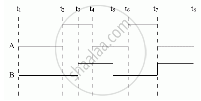
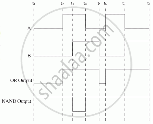
Show the output waveforms (Y) for the following inputs A and B of (i) OR gate (ii) NAND gate ?

Advertisements

Solution

 Output waveforms (Y)

shaalaa.com
  Is there an error in this question or solution?
2011-2012 (March) Delhi Set 1

RELATED QUESTIONS

If a small voltage is applied to a p-n junction diode, how will the barrier potential be affected when it is(ii) reveres biased?


How is a photodiode fabricated?


Briefly explain its working. Draw its V - I characteristics for two different intensities of illumination ?


Draw the circuit diagram of a full wave rectifier using p-n junction diode.

Explain its working and show the output, input waveforms.


An ideal diode should pass a current freely in one direction and should stop it completely in the opposite direction. Which is closer to ideal-vacuum diode or a p-njunction diode?


Draw the V-I characteristics of an LED. State two advantages of LED lamps over convertional  incandescent lamps. 


Write the important considerations which are to be taken into account while fabricating a p-n junction diode to be used as a Light Emitting Diode (LED). What should be the order of the band gap of an LED, if it is required to emit light in the visible range? Draw a circuit diagram and explain its action.


Consider the following statements (A) and (B) and identify the correct answer.

  1. A Zener diode is connected in reverse bias when used as a voltage regulator.
  2. The potential barrier of the p-n junction lies between 0.1 V to 0.3 V.

The value of power dissipated across the Zener diode (Vz = 15 V) connected in the circuit as shown in the figure is x × 10–1 watt. The value of x, to the nearest integer, is ______.


Identify the special purpose diodes 'A', 'B' and 'C' from the given symbols.


Share
Notifications

Englishहिंदीमराठी


      Forgot password?
Use app×