Advertisements
Advertisements
प्रश्न
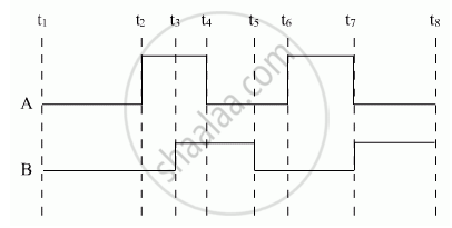
Show the output waveforms (Y) for the following inputs A and B of (i) OR gate (ii) NAND gate ?

Advertisements
उत्तर
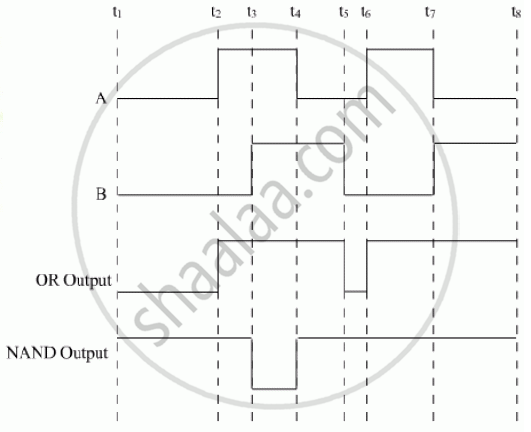
Output waveforms (Y)

APPEARS IN
संबंधित प्रश्न
If a small voltage is applied to a p-n junction diode, how will the barrier potential be affected when it is(ii) reveres biased?
Using the necessary circuit diagrams, show how the V-I characteristics of a p-n junction are obtained in
Reverse biasing
How are these characteristics made use of in rectification?
Describe, with the help of a circuit diagram, the working of a photodiode.
Why is zener diode fabricated by heavily doping both p- and n-sides of the junction?
Explain the formation of depletion layer and potential barrier in a p−n junction.
Draw the V-I characteristics of an LED. State two advantages of LED lamps over convertional incandescent lamps.
The wavelength and intensity of light emitted by a LED depend upon ______.
Which one of the following is not the advantage of LED?
Read the following paragraph and answer the questions.
|
LED is a heavily doped P-N junction which under forward bias emits spontaneous radiation. When it is forward-biased, due to recombination of holes and electrons at the junction, energy is released in the form of photons. In the case of Si and Ge diode, the energy released in recombination lies in the infrared region. LEDs that can emit red, yellow, orange, green and blue light are commercially available. The semiconductor used for fabrication of visible LEDs must at least have a band gap of 1.8 eV. The compound semiconductor Gallium Arsenide – Phosphide is used for making LEDs of different colours.
|
- Why are LEDs made of compound semiconductor and not of elemental semiconductors?
- What should be the order of bandgap of an LED, if it is required to emit light in the visible range?
- A student connects the blue coloured LED as shown in the figure. The LED did not glow when switch S is closed. Explain why?

OR
iii. Draw V-I characteristic of a p-n junction diode in
(i) forward bias and (ii) reverse bias
The value of power dissipated across the Zener diode (Vz = 15 V) connected in the circuit as shown in the figure is x × 10–1 watt. The value of x, to the nearest integer, is ______.


