Advertisements
Advertisements
Question
With reference to Semiconductor Physics,
Name the process that causes depletion region in a p-n junction.
Advertisements
Solution
Diffusion of electrons of n-type crystal into holes of p-type crystal.
APPEARS IN
RELATED QUESTIONS
Colour of light emitted by LED depends upon__________________ .
- its forward bias
- its reverse bias
- the band gap of the material of semiconductor
- its size
The width of depletion region of p-n junction diode is _______.
(A) 0.5 nm to 1 nm
(B) 5 nm to 10 nm
(C) 50 nm to 500 nm
(D) 500 nm to 1000 nm
Write briefly the important processes that occur during the formation of p−n junction. With the help of necessary diagrams, explain the term 'barrier potential'.
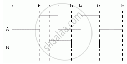
Show the output waveforms (Y) for the following inputs A and B of (i) OR gate (ii) NAND gate ?
What is a solar cell?
Draw solar cell V-I characteristics.
A p-n photodiode is fabricated from a semiconductor with a band gap of 2.5 eV. lt can detect a signal of wavelength ______.
Which one of the following is not the advantage of LED?
Consider the following statements (A) and (B) and identify the correct answer.
- A Zener diode is connected in reverse bias when used as a voltage regulator.
- The potential barrier of the p-n junction lies between 0.1 V to 0.3 V.
How can a photodiode be used to measure light intensity?
