Advertisements
Advertisements
Question
With the help of a neat circuit diagram, explain the working of a photodiode.
Advertisements
Solution

a. A photodiode is a special purpose P-N junction diode fabricated with a transparent window to allow light to fall on the diode.
b. When the photodiode is illuminated with light (photons) with energy h greater than the energy gap Eg of the semiconductor, then electron-hole pairs are generated due to the absorption of photons.
c. The diode is fabricated such that the generation of electron-hole pairs takes place in or near the depletion region of the diode.
d. Due to electric field of the junction, electrons and holes are separated before they recombine.
e. The direction of the electric field is such that electrons reach N-side and holes reach Pside. Electrons are collected on N-side and holes are collected on P-side giving rise to an e.m.f.
f. When an external load is connected, current flows. The magnitude of the photocurrent depends on the intensity of incident light.
g. It is easier to observe the change in the current with change in the light intensity, if a reverse bias is applied. Thus, photodiode can be used as a photodetector to detect optical signals.
RELATED QUESTIONS
Colour of light emitted by LED depends upon__________________ .
- its forward bias
- its reverse bias
- the band gap of the material of semiconductor
- its size
Meeta's father was driving her to school. At the traffic signal, she noticed that each traffic light was made of many tiny lights instead of a single bulb. When Meeta asked this question to her father, he explained the reason for this.
Answer the following questions based on above information:
(i) What were the values displayed by Meeta and her father?
(ii) What answer did Meeta's father give?
(iii) What are the tiny lights in traffic signals called and how do these operate?
How is a Zener diode fabricated?
Explain with the help of a diagram, how depletion region and potential barrier are formed in a junction diode.
If a small voltage is applied to a p-n junction diode, how will the barrier potential be affected when it is (i) forward biased
If a small voltage is applied to a p-n junction diode, how will the barrier potential be affected when it is(ii) reveres biased?
With what considerations in view, a photodiode is fabricated? State its working with the help of a suitable diagram.
Even though the current in the forward bias is known to be more than in the reverse bias, yet the photodiode works in reverse bias. What is the reason?
Using the necessary circuit diagrams, show how the V-I characteristics of a p-n junction are obtained in
Forward biasing
How are these characteristics made use of in rectification?
A p-n photodiode is fabricated from a semiconductor with band gap of 2.8 eV. Can it detect a wavelength of 6000 nm?
The width of depletion region of p-n junction diode is _______.
(A) 0.5 nm to 1 nm
(B) 5 nm to 10 nm
(C) 50 nm to 500 nm
(D) 500 nm to 1000 nm
State its any ‘two’ uses of photodiode.
Describe, with the help of a circuit diagram, the working of a photodiode.
How is a photodiode fabricated?
Briefly explain its working. Draw its V - I characteristics for two different intensities of illumination ?
Draw the circuit diagram of a full wave rectifier using p-n junction diode.
Explain its working and show the output, input waveforms.
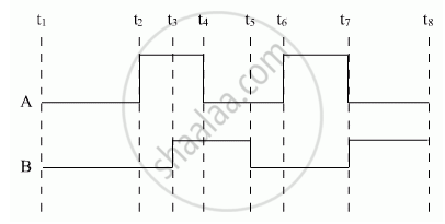
Show the output waveforms (Y) for the following inputs A and B of (i) OR gate (ii) NAND gate ?
Describe briefly, with the help of a diagram, the role of the two important processes involved in the formation of a p-n junction.
Draw the circuit diagram of an illuminated photodiode in reverse bias. How is photodiode used to measure light intensity?
Explain how a potential barrier is developed in a p-n junction diode.
Draw the V-I characteristics of an LED. State two advantages of LED lamps over convertional incandescent lamps.
What is a solar cell?
Draw solar cell V-I characteristics.
Explain the three processes involved in the working of a solar cell.
With reference to Semiconductor Physics,
Name the process that causes depletion region in a p-n junction.
What is the magnitude of the potential barrier across a Ge p-n junction?
Name the device which converts the change in intensity of illumination to change in electric current flowing through it. Plot I-V characteristics of this device for different intensities. State any two applications of this device.
For LED's to emit light in visible region of electromagnetic light, it should have energy band gap in the range of:
Which one of the following is not the advantage of LED?
Consider the following statements (A) and (B) and identify the correct answer.
- A Zener diode is connected in reverse bias when used as a voltage regulator.
- The potential barrier of the p-n junction lies between 0.1 V to 0.3 V.
In Figure, assuming the diodes to be ideal ______.

The amplifiers X, Y and Z are connected in series. If the voltage gains of X, Y and Z are 10, 20 and 30, respectively and the input signal is 1 mV peak value, then what is the output signal voltage (peak value)
- if dc supply voltage is 10V?
- if dc supply voltage is 5V?
If the resistance R1 is increased (Figure), how will the readings of the ammeter and voltmeter change?

Read the following paragraph and answer the questions.
|
LED is a heavily doped P-N junction which under forward bias emits spontaneous radiation. When it is forward-biased, due to recombination of holes and electrons at the junction, energy is released in the form of photons. In the case of Si and Ge diode, the energy released in recombination lies in the infrared region. LEDs that can emit red, yellow, orange, green and blue light are commercially available. The semiconductor used for fabrication of visible LEDs must at least have a band gap of 1.8 eV. The compound semiconductor Gallium Arsenide – Phosphide is used for making LEDs of different colours.
|

- Why are LEDs made of compound semiconductor and not of elemental semiconductors?
- What should be the order of bandgap of an LED, if it is required to emit light in the visible range?
- A student connects the blue coloured LED as shown in the figure. The LED did not glow when switch S is closed. Explain why?

OR
iii. Draw V-I characteristic of a p-n junction diode in
(i) forward bias and (ii) reverse bias
Why a photo-diode is operated in reverse bias whereas the current in the forward bias is much larger than that in the reverse bias? Explain. Mention its two uses.
Briefly explain how emf is generated in a solar cell.
Draw solar cells of I-V characteristics.
Draw the circuit diagram of an illuminated photodiode and its I-V characteristics.
How can a photodiode be used to measure light intensity?
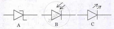
Identify the special purpose diodes 'A', 'B' and 'C' from the given symbols.
Select the wrong statement in the case of LED.
Consider the following statements A and B and identify the correct answer:
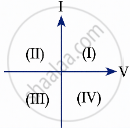
- For a solar-cell the I-V characteristics lies in the (IV) quadrant of the given graph.
- In a reverse biased p-n junction diode, the current measured in (μA), is due to majority charge carriers.
Consider the following statements A and B and identify the correct answer:
- For a solar-cell, the I-V characteristics lies in the IV quadrant of the given graph.
- In a reverse biased pn junction diode, the current measured in (A), is due to majority charge carriers.
