Advertisements
Advertisements
Question
Describe, with the help of a circuit diagram, the working of a photodiode.
Advertisements
Solution
Photo diode is a p-n junction diode made of photosensitive semiconductor in which current carriers are generated by photons through photo excitation, i.e., photo conduction by light. It is operated under reverse bias below the breakdown voltage.

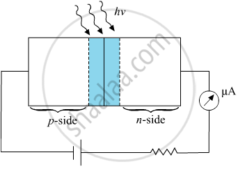
Working of Photo diode
- The diode is fabricated such that the generation of e-h pairs takes place in or near the depletion region of the diode.
When visible light of energy greater than forbidden energy gap ( \[h\nu > E_g\] ) is incident on a reverse bias p-n junction photo diode, additional electron-hole pairs are created in the depletion region ( or near the Junction).
- These charge carriers will be separated by the junction and made to flow across the junction, creating a reverse current across the junction.
- The direction of the electric field is such that electrons reach n-side and holes are
- The value of reverse saturation current increases with the increase in the intensity of incident light as shown here. Hence, thereverse saturation current through the photo diode varies linearly with the light intensity.
- collected on p-side giving rise to an emf.
I – V characteristics of photo diode

APPEARS IN
RELATED QUESTIONS
Colour of light emitted by LED depends upon__________________ .
- its forward bias
- its reverse bias
- the band gap of the material of semiconductor
- its size
Explain with the help of a diagram, how depletion region and potential barrier are formed in a junction diode.
Why is zener diode fabricated by heavily doping both p- and n-sides of the junction?
Draw V − I characteristics of a p-n junction diode. Answer the following questions, giving reasons:
(i) Why is the current under reverse bias almost independent of the applied potential up to a critical voltage?
(ii) Why does the reverse current show a sudden increase at the critical voltage?
Name any semiconductor device which operates under the reverse bias in the breakdown region.
The current in the forward bias is known to be more (~mA) than the current in the reverse bias (~μA). What is the reason, then, to operate the photodiode in reverse bias?
Show the output waveforms (Y) for the following inputs A and B of (i) OR gate (ii) NAND gate ?

What happens to the width of depletion player of a p-n junction when it is (i) forward biased, (ii) reverse biased?
Write the important considerations which are to be taken into account while fabricating a p-n junction diode to be used as a Light Emitting Diode (LED). What should be the order of band gap of an LED, if it is required to emit light in the visible range? Draw a circuit diagram and explain its action.
If the resistance R1 is increased (Figure), how will the readings of the ammeter and voltmeter change?

Select the wrong statement in the case of LED.
