Advertisements
Advertisements
Question
Draw V − I characteristics of a p-n junction diode. Answer the following questions, giving reasons:
(i) Why is the current under reverse bias almost independent of the applied potential up to a critical voltage?
(ii) Why does the reverse current show a sudden increase at the critical voltage?
Name any semiconductor device which operates under the reverse bias in the breakdown region.
Advertisements
Solution
V-I characteristic of p-n junction diode:
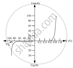
(i) Under the reverse bias condition, the holes of p-side are attracted towards the negative terminal of the battery and the electrons of the n-side are attracted towards the positive terminal of the battery. This increases the depletion layer and the potential barrier. However the minority charge carriers are drifted across the junction producing a small current. At any temperature the number of minority carriers is constant so there is the small current at any applied potential. This is the reason for the current under reverse bias to be almost independent of applied potential. At the critical voltage, avalanche breakdown takes place which results in a sudden flow of large current.
(ii) At the critical voltage, the holes in the n-side and conduction electrons in the p-side are accelerated due to the reverse −bias voltage. These minority carriers acquire sufficient kinetic energy from the electric field and collide with a valence electron. Thus the bond is finally broken and the valence electrons move into the conduction band resulting in enormous flow of electrons and thus formation of hole-electron pairs. Thus there is a sudden increase in the current at the critical voltage.
Zener diode is a semiconductor device which operates under the reverse bias in the breakdown region.
