Advertisements
Advertisements
Question
The logic gate which produces LOW output when one of the input is HIGH and produces
HIGH output only when all of its inputs are LOW is called _______.
(A) AND gate
(B) OR gate
(C) NOR gate
(D) NAND gate
Advertisements
Solution
(C) NOR gate
APPEARS IN
RELATED QUESTIONS
Which logic gate corresponds to the truth table given below?
|
A |
B |
Y |
|
0 |
0 |
I |
|
0 |
1 |
0 |
|
1 |
0 |
0 |
|
1 |
1 |
0 |
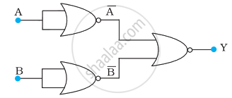
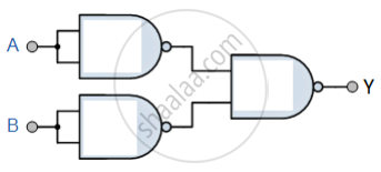
You are given the two circuits as shown in following figure. Show that circuit
- acts as OR gate while the circuit
- acts as AND gate.
(a)
(b)
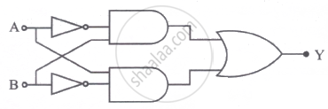
Write the truth table for the circuits given in following figure consisting of NOR gates only. Identify the logic operations (OR, AND, NOT) performed by the two circuits.
(a)
(b)
Draw logic symbol of an OR gate and write its truth table.
Answer the following question :
Distinguish between digital and analogue signals.
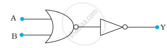
You are given a circuit below. Write its truth table. Hence, identify the logic operation carried out by this circuit. Draw the logic symbol of the gate it corresponds to.
The output of an OR gate is connected to both the inputs of a NAND gate Draw the logic circuit of this combinaion of getes and write its truth table.
Why is the linear portion of the triode characteristic chosen to operate the triode as an amplifier?
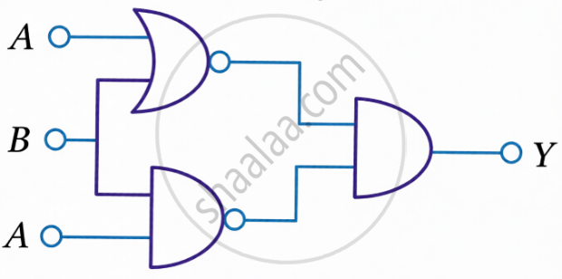
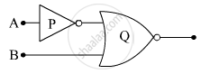
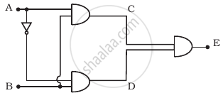
(i) Write the truth tables of the logic gates marked P and Q in the given circuit.
(ii) Write the truth table for the circuit.
Why are NOR gates considered as universal gates?
Show the variation of voltage with time, for a digital signal.
Draw a diagram to show how NAND gates can be combined to obtain an OR gate. (Truth table is not, required)
Useful Constants and Relations:
| 1. | Charge of a proton | (e) | =1.6 × 10⁻¹⁹C |
| 2. | Planck's constant | (h) | = 6·6 × 10-34 Js |
| 3. | Mass of an electron | (m) | = 9·1× 10-31 kg |
| 4. | Permittivity of vacuum | (∈0) | =8 · 85 × 10-12 Fm-1 |
| 5. | `(1/(4pi∈_0))` | =9 ×10⁹ mF-1 | |
| 6. | Permeability of vacuum | (μ0) | = 4π × 10-7 Hm-1 |
| 7. | `((mu_0)/(4pi))` | =1 × 10⁻⁷ Hm-1 | |
| 8. | Speed of light in vacuum | (c) | = 3× 10⁸ ms-1 |
| 9. | Unified atomic mass unit | (u) |
= 931 MeV |
| 10. | Electron volt | (leV) | = 1.6 × 10⁻¹⁹ J |
The outputs of two NOT gates are fed to a NOR gate. Draw the logic circuit of the combination of gates. Write its truth table. Identify the gate equivalent to this circuit.
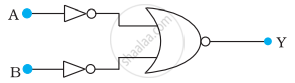
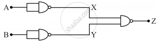
You are given circuit as shown in the figure, which consists of NAND gate. Identify the logic operation carried out by the two. Write the truth table. Identify the gates equivalent to the tow circuits.
You are given a circuit as shown in the figure, which consists of the NAND gate. Identify the logic operation carried out by the two. Write the truth table. Identify the gates equivalent to the tow circuit.
The output of 2-input or gate is zero only when its
An oscillator is nothing but an amplifier with
In potential barrier development in a junction diode opposes
The truth table for the following logic circuit is:
For the given circuit, the input digital signals are applied at the terminals A, B and C. What would be the output at the terminal y?

Truth table for the given circuit (Figure) is ______.
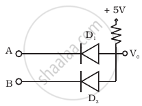
Two car garages have a common gate which needs to open automatically when a car enters either of the garages or cars enter both. Devise a circuit that resembles this situation using diodes for this situation.
How would you set up a circuit to obtain NOT gate using a transistor?
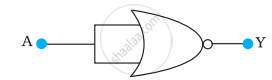
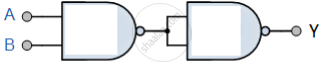
Write the truth table for the circuit shown in figure. Name the gate that the circuit resembles.
Draw the output signals C1 and C2 in the given combination of gates (Figure).


The output (Y) of the given logic implementation is similar to the output of an/a ______ gate.