Advertisements
Advertisements
Question
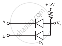
Write the truth table for the circuit shown in figure. Name the gate that the circuit resembles.
Advertisements
Solution
This is ‘AND’ Gate and its characteristics are as follows:
(1) It has two inputs (A and B) and only one output (Y).
(2) Boolean expression us Y = A·B is read as "Y equals A AND B".
(3) Realization of AND gate

Logical symbol of AND gate

(i) A = 0, 8 = 0
The voltage supply through R is forward biasing diodes D1 and D2 (offers low resistance), the voltage V would drop across R. The output voltage at Y = the voltage across diode = 0
(ii) A = 0, B = 1
D1 = Conducts, D2 = Not Conducts
The out voltage at Y = The voltage across the diode (D1) = 0
(iii) A = 1, B = 0
D1 = Conducts, D2 = Not conducts
The out voltage at Y = The voltage across the diode (D2) = 0
(iv) A = 1, B = 1
None of the diode conducts
The out voltage at Y = Battery voltage = 1
(4) Truth table for ‘AND’ gate
| A | B | V0 = A · B |
| 0 | 0 | 0 |
| 0 | 1 | 0 |
| 1 | 0 | 0 |
| 1 | 1 | 1 |
