Advertisements
Advertisements
Question
How would you set up a circuit to obtain NOT gate using a transistor?
Advertisements
Solution
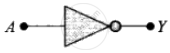
(1) It has only one input and only one output.
(2) Boolean expression is Y = Ᾱ and is read as “y equals not A”.
Logical symbol of NOT gate.

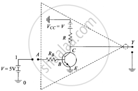
(3) Realization of NOT gate: The transistor is so biased that the collector voltage VCC = V (Voltage corresponding to 1 state)
The resistors R and RB are so chosen that if the input is low, i.e. 0, the transistor is in the cut-off and hence the voltage appearing at the output will be the same as applied V = 5 V. Hence Y = V (or state I)
If the input is high, the transistor current is in saturation and the net voltage at the output Y is 0 (in state 0).

(4) Truth table for NOT gate:
| A | Y = Ā |
| 0 | 1 |
| 1 | 0 |
APPEARS IN
RELATED QUESTIONS
Identify the logic gates marked 'P' and 'Q' in the given circuit. Write the truth table for the combination.

The logic gate which produces LOW output when one of the input is HIGH and produces
HIGH output only when all of its inputs are LOW is called _______.
(A) AND gate
(B) OR gate
(C) NOR gate
(D) NAND gate
You are given two circuits as shown in following figure, which consist of NAND gates. Identify the logic operation carried out by the two circuits.
(a)

(b)

Write the truth table for circuit given in figure below consisting of NOR gates and identify the logic operation (OR, AND, NOT) which this circuit is performing.

(Hint: A = 0, B = 1 then A and B inputs of second NOR gate will be 0 and hence Y=1. Similarly work out the values of Y for other combinations of A and B. Compare with the truth table of OR, AND, NOT gates and find the correct one.)
Draw logic symbol of an OR gate and write its truth table.
Identify the logic gate represented by the circuit as shown and write its truth table.

Name the logic gate which generated high output when at least one input is high.
Let \[X = A \overline{ BC} + B\overline{ CA} + C\overline{AB } .\] Evaluate X for A = 1, B = 0, C = 1.
Let \[X = A \overline{ BC} + B\overline{ CA} + C\overline{AB } .\] Evaluate X for A = B = C = 0.
Show that \[AB + \overline {AB }\] is always 1.
(i) Write the truth tables of the logic gates marked P and Q in the given circuit.
(ii) Write the truth table for the circuit.

Why are NOR gates considered as universal gates?
A radar is sending out pules of 1 micro second duration at interval of 100 micro-second. The range of the radar is
In potential barrier development in a junction diode opposes
For the given circuit, the input digital signals are applied at terminals A, B, and C. What would be the output at terminal y?


For the given circuit, the input digital signals are applied at the terminals A, B and C. What would be the output at the terminal y?

Two car garages have a common gate which needs to open automatically when a car enters either of the garages or cars enter both. Devise a circuit that resembles this situation using diodes for this situation.
An X-OR gate has following truth table:
| A | B | Y |
| 0 | 0 | 0 |
| 0 | 1 | 1 |
| 1 | 0 | 1 |
| 1 | 1 | 0 |
It is represented by following logic relation `Y = barA.B + A.barB`. Build this gate using AND, OR and NOT gates.
Which of the following gives a reversible operation?
A logic circuit provides the output Y as per the following truth table:
| A | B | Y |
| 0 | 0 | 1 |
| 0 | 1 | 0 |
| 1 | 0 | 1 |
| 1 | 1 | 0 |
The expression for the output Y is:
