Advertisements
Advertisements
Question
The output of an OR gate is connected to both the inputs of a NAND gate Draw the logic circuit of this combinaion of getes and write its truth table.
Advertisements
Solution 1
Both the inputs of the NAND gates are joined to form a single input. Therefore, it behaves like a NOT gate.
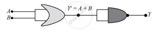
| A | B | A + B | `overline(A+B)` |
| 0 | 0 | 0 | 1 |
| 0 | 1 | 1 | 0 |
| 1 | 0 | 1 | 0 |
| 1 | 1 | 1 | 0 |
shaalaa.com
Solution 2
Both the inputs of the NAND gates are joined to form a single input. Therefore, it behaves like a NOT gate.
| A | B | A + B | `overline(A+B)` |
| 0 | 0 | 0 | 1 |
| 0 | 1 | 1 | 0 |
| 1 | 0 | 1 | 0 |
| 1 | 1 | 1 | 0 |
shaalaa.com
Is there an error in this question or solution?
