Advertisements
Advertisements
Question
(i) Write the truth tables of the logic gates marked P and Q in the given circuit.
(ii) Write the truth table for the circuit.
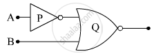
Advertisements
Solution
(i) P and Q are the NOT and OR gates respectively. The truth table for them is drawn below:
| NOT | OR | |||
|---|---|---|---|---|
| Input | Output | Input 1 | Input 2 | Output |
| 1 | 0 | 1 | 1 | 1 |
| 0 | 1 | 0 | 0 | 0 |
| 1 | 0 | 1 | ||
| 0 | 1 | 1 | ||
(ii) The truth table for the whole network:
| Input -A | Input -B | Output |
|---|---|---|
| 1 | 1 | 1 |
| 0 | 0 | 1 |
| 1 | 0 | 0 |
| 0 | 1 | 1 |
RELATED QUESTIONS
Write the truth table for the circuits given in following figure consisting of NOR gates only. Identify the logic operations (OR, AND, NOT) performed by the two circuits.
(a)

(b)

Draw the schematic symbols for AND, OR, NOT and NAND gate
The output of an OR gate is connected to both the inputs of a NAND gate Draw the logic circuit of this combinaion of getes and write its truth table.
Why are NOR gates considered as universal gates?
The outputs of two NOT gates are fed to a NOR gate. Draw the logic circuit of the combination of gates. Write its truth table. Identify the gate equivalent to this circuit.
The output of 2-input or gate is zero only when its
Draw the output signals C1 and C2 in the given combination of gates (Figure).


A logic gate circuit has two inputs A and B and output Y. The voltage waveforms of A, B and Y are shown below.

The logic gate circuit is ______.
A logic circuit provides the output Y as per the following truth table:
| A | B | Y |
| 0 | 0 | 1 |
| 0 | 1 | 0 |
| 1 | 0 | 1 |
| 1 | 1 | 0 |
The expression for the output Y is:
The output (Y) of the given logic implementation is similar to the output of an/a ______ gate.

