Advertisements
Advertisements
Question
Draw the circuit symbol of the PNP transistor.
Advertisements
Solution
The circuit symbol of the p-n-p transistor

APPEARS IN
RELATED QUESTIONS
Why is the base of a transistor made thin and is lightly doped?
Explain the working of the PNP transistor?
Draw the circuit symbol for NPN and PNP transistors. What is the difference in the Emitter, Base, and Collector regions of a transistor?
With the help of a neat circuit diagram, explain the transistor as an amplifier?
The principle based on which a solar cell operates is ____________.
The light emitted in an LED is due to
What is rectification?
Describe the function of a transistor as an amplifier with the neat circuit diagram. Sketch the input and output wave forms.
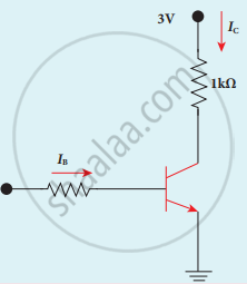
Assuming VCEsat = 0.2 V and β = 50, find the minimum base current (IB) required to drive the transistor given in the figure to saturation.
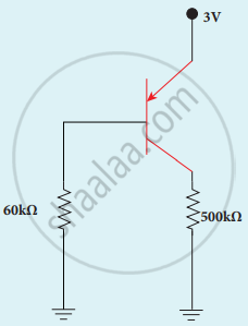
In the circuit shown in the figure, the BJT has a current gain (β) of 50. For an emitter-base voltage VEB = 600 mV, calculate the emitter-collector voltage VEC (in volts).
A transistor has a voltage gain A. If the amount βA of its output is applied to the input of the transistor, then the transistor becomes oscillator, when ______.
A common emitter amplifier is designed with n-p-n transistor (α = 0.99). The input impedance is 1 kΩ and the load is 10 kΩ. The voltage gain will be ______
For a transistor, the current ratio 'βdc' is defined as the ratio of ______.
In the symbol for a transistor, the arrow head points in the direction of the ____________.
In a transistor in CE configuration, the ratio of power gain to voltage gain is ____________.
In switching circuit, transistor is in ON state, values of IE and lB are 10 mA and 0.8 mA respectively and RL is 2 k`Omega`. If VCE is 7.6 V, then VCC is ____________.
Which of the following regions of a transistors are, respectively, heavily dopped and lightly dopped?
In case of npn transistors, the collector current is always less than the emitter current because ______.
For a common emitter configuration, if 'α' and 'β' have their usual meanings, the correct relationship between 'α' and 'β' is ______.
In a transistor, a change of 8.0 mA in the emitter current produces a change of 7.8 mA in the collector current. Then change in the base current is ____________.
A transistor when connected in common emitter mode has a ____________.
A pnp transistor is used in common-emitter mode. If a change of 40 µA in base current brings a change of 2 µA in collector current with 0.04 V in base-emitter voltage, then the input resistance is ____________.
In common emitter mode of transistor, the d.c. current gain is 20, the emitter current is 7 mA. The collector current is ______.
The reverse bias in a junction diode is changed from 8V to 13V, then the value of the current changes from 40μA to 60μA. The resistance of junction diode will be ______.
The transfer ratio of a transistor is 50. The input resistance of the transistor when used in the CE configuration is 1K Ω. The peak value for an AC input voltage of 0.01 V of collector current is ______.
Explain the working of the n-p-n transistor in a common base configuration.
The collector current in a common-emitter transistor amplifier is 4 mA. When the base current is increased by 20 µA, the collector current increases to 6 mA. The current gain is ______.
Define α.
When an n-p-n junction transistor is used as an amplifier in common emitter mode, ______.
