Advertisements
Advertisements
Question
Draw the circuit diagram to study the characteristic of the transistor in common emitter mode. Draw the input and output characteristics.
Advertisements
Solution
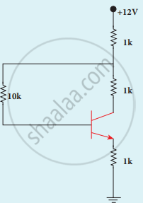
- Circuit to study Common Emitter (CE) characteristic:

- The Input characteristics:

- The output characteristics:

APPEARS IN
RELATED QUESTIONS
Why are the emitter, the base, and the collector of a BJT doped differently?
Derive the relation between α and β.
Draw the circuit symbol of the PNP transistor.
With the help of a neat diagram, explain the working of the npn transistor?
The output of the following circuit is 1 when the input ABC is
Describe the function of a transistor as an amplifier with the neat circuit diagram. Sketch the input and output wave forms.
A transistor of α = 0.99 and VBE = 0.7 V is connected in the common-emitter configuration as shown in the figure. If the transistor is in the saturation region, find the value of collector current.
A transistor has a voltage gain A. If the amount βA of its output is applied to the input of the transistor, then the transistor becomes oscillator, when ______.
A common emitter amplifier is designed with n-p-n transistor (α = 0.99). The input impedance is 1 kΩ and the load is 10 kΩ. The voltage gain will be ______
The condition to convert an amplified signal into an oscillating signal is ______
A transistor having α = 0.8 is connected in common emitter configuration. When the base current changes by 6 mA, then the change in collector current is ______.
If l1, l2, l3 are the lengths of the emitter, base and collector of a transistor, then ____________.
Least doped region in a transistor ____________.
In an npn transistor, the collector current is 24 mA. If 80% of electrons reach collector, its base current in mA is ______.
In a transistor in CE configuration, the ratio of power gain to voltage gain is ____________.
Which of the following regions of a transistors are, respectively, heavily dopped and lightly dopped?
In case of npn transistors, the collector current is always less than the emitter current because ______.
In a transistor, doping level in base is increased slightly, the collector current and base current respectively ______.
In common emitter mode of transistor, the d.c. current gain is 20, the emitter current is 7 mA. The collector current is ______.
A change of 9.0 mA in the emitter current brings a change of 8.9 mA in the collector current. The value of current gain β will be ______.
A transistor having α = 0.8 is connected in a common emitter configuration. When the base current changes by 6 mA, the change in collector current is ______
A transistor is used as a common emitter amplifier with a load resistance 2 KΩ. The input resistance is 150 Ω. Base current is changed by 20 µA which results in a change in collector current by 1.5 mA. The voltage gain of the amplifier is ______.
A conducting wire has length 'L1' and diameter 'd1'. After stretching the same wire length becomes 'L2' and diameter 'd2' The ratio of resistances before and after stretching is ______.
The reverse bias in a junction diode is changed from 8V to 13V, then the value of the current changes from 40μA to 60μA. The resistance of junction diode will be ______.
The transfer ratio of a transistor is 50. The input resistance of the transistor when used in the CE configuration is 1K Ω. The peak value for an AC input voltage of 0.01 V of collector current is ______.
How is a transistor biased for operating it as amplifier?
For a common emitter transistor configuration the ratio of `I_c/I_E` = 0.96, then the current gain in this configuration is ______.
