Advertisements
Advertisements
Question
Why are the emitter, the base, and the collector of a BJT doped differently?
Advertisements
Solution
A BJT is a bipolar device, both electrons and holes participate in the conduction process. Under the forward-biased condition, the majority of carriers injected from the emitter into the base constitute the largest current component in a BJT. For these carriers to diffuse across the base region with negligible recombination and reach the collector junction, they must overwhelm the majority of carriers of the opposite charge in the base. The total emitter current has two components, due to majority carriers in the emitter and due to minority carriers diffusing from the base into the emitter. The ratio of the current component due to the injected majority carriers from the emitter to the total emitter current is a measure of the emitter efficiency. To improve the emitter efficiency and the common-base current gain (α), it can be shown that the emitter should be much more heavily doped than the base.
Also, the base width is a function of the base-collector voltage. A low doping level of the collector increases the size of the depletion region. This increases the maximum collector-base voltage and reduces the base width. Further, the large depletion region at the collector-base junction-extending mainly into the collector-corresponds to a smaller electric field and avoids avalanche breakdown of the reverse-biased collector-base junction.
[Note: Effective dopant concentrations of (a) npn transistor (b) pnp transistor are shown below.]
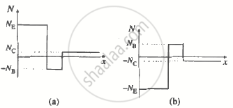
The base doping is less than the emitter doping but greater than the collector doping.
RELATED QUESTIONS
Which method of biasing is used for operating a transistor as an amplifier?
In a common base configuration, the transistor has an emitter current of 10 mA and a collector current of 9.8 mA. The value of base current is ______
With the help of a neat circuit diagram, explain the transistor as an amplifier?
The principle based on which a solar cell operates is ____________.
Give the Barkhausen conditions for sustained oscillations.
Explain the current flow in an NPN transistor.
Describe the function of a transistor as an amplifier with the neat circuit diagram. Sketch the input and output wave forms.
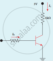
Assuming VCEsat = 0.2 V and β = 50, find the minimum base current (IB) required to drive the transistor given in the figure to saturation.
The condition to convert an amplified signal into an oscillating signal is ______
For a transistor, the current ratio 'βdc' is defined as the ratio of ______.
In switching circuit, transistor is in ON state. Values of IC and IB are 5.2 mA and 10 µA respectively and value of RC is 1 k`Omega`. If Vcc is at 5.5 V, then VCE is ______.
Ve, Vb, and Ve are emitter, base, and collector voltage respectively for npn transistor in CE mode. Amplifier works for the combination of biasing voltage equal to ______.
If `alpha`-current gain of a transistor is 0.98. What is the value of `beta`- current gain of the transistor?
For a common emitter configuration, if 'α' and 'β' have their usual meanings, the correct relationship between 'α' and 'β' is ______.
In transistor amplifier, base-emitter junction is forward biased and collector emitter junction is reverse biased. The current gain is ______.
In the case of transistor, the relation between current ratios αdc and βdc is ______.
In common emitter mode of transistor, the d.c. current gain is 20, the emitter current is 7 mA. The collector current is ______.
A transistor is connected in C - E mode. If collector current is 72 × 10-5 A and α = 0.96, then base current will be ______.
For an ideal diode, the current in the following arrangement is ______.

A transistor having α = 0.8 is connected in a common emitter configuration. When the base current changes by 6 mA, the change in collector current is ______
In a p-n-p transistor circuit, the collector current is 10 mA. If 90% of the holes emitted from the emitter reach the collector, ______.
The reverse bias in a junction diode is changed from 8V to 13V, then the value of the current changes from 40μA to 60μA. The resistance of junction diode will be ______.
The current amplification factor for a transistor in its common emitter mode is 50. The current amplification factor in the common base mode of the transistor is ______.
Explain the working of the n-p-n transistor in a common base configuration.
The collector current in a common-emitter transistor amplifier is 4 mA. When the base current is increased by 20 µA, the collector current increases to 6 mA. The current gain is ______.
Explain the output characteristics of common emitter configuration of n-p-n transistor.
Define α.
When an n-p-n junction transistor is used as an amplifier in common emitter mode, ______.
