Advertisements
Advertisements
Question
Explain the working of the PNP transistor?
Advertisements
Solution
Working of p-n-p transistor:
- The majority of charge carriers in the emitter of the p-n-p transistor are holes.
- A typical biasing of a transistor is shown in figure (a). In this, the emitter-base junction is forward biased while the collector-base junction is reverse biased.

Figure (a) - At the instant when the EB junction is forward biased, holes in the emitter region have not entered the base region as shown in figure (b).
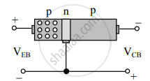
Figure (b) - When the biasing voltage VBE is greater than the barrier potential (0.6 – 0.7 V for Si transistors), many holes enter the base region and form the emitter current IE as shown in figure (c).

Figure (c) - These holes can either flow through the base circuit and constitute the base current (IB), or they can also flow through the collector circuit and contribute towards the collector current (IC).
- The base is thin and lightly doped, the base current is only 5% of IE.
- Holes injected from the emitter into the base diffuse into the collector-base depletion region due to the thin base region. When the holes enter the collector-base depletion region, they are pushed into the collector region by the electric field at the collector-base depletion region. The collector current (IC) flows through the external circuit as shown in figure (d). The collector's current IC is about 95% of IE.

Figure (d)
From the figure, we can conclude that IE = IB + IC Since the base current IB is very small we can write IC ≈ IE.
APPEARS IN
RELATED QUESTIONS
In a BJT, the largest current flow occurs ______.
Why are the emitter, the base, and the collector of a BJT doped differently?
For a transistor β =75 and IE = 7.5 mA. The value of α is ______
Draw the circuit diagram to study the characteristic of the transistor in common emitter mode. Draw the input and output characteristics.
The principle based on which a solar cell operates is ____________.
Give the Barkhausen conditions for sustained oscillations.
What is rectification?
Sketch the static characteristics of a common emitter transistor and bring out the essential features of input and output characteristics.
Describe the function of a transistor as an amplifier with the neat circuit diagram. Sketch the input and output wave forms.
A transistor has a voltage gain A. If the amount βA of its output is applied to the input of the transistor, then the transistor becomes oscillator, when ______.
The condition to convert an amplified signal into an oscillating signal is ______
Least doped region in a transistor ____________.
In a transistor in CE configuration, the ratio of power gain to voltage gain is ____________.
In an npn transistor circuit, the collector current is 10 mA. If 90% of the electrons emitted reach the collector, the emitter current (IE) and base current (IB) are given by ____________.
A pnp transistor is used in common-emitter mode. If a change of 40 µA in base current brings a change of 2 µA in collector current with 0.04 V in base-emitter voltage, then the input resistance is ____________.
The current gain `alpha` of a transistor is 0.95. The change in collector current corresponding to a change of 0.4 mA in the base current in a common emitter arrangement is ______.
A transistor is connected in C - E mode. If collector current is 72 × 10-5 A and α = 0.96, then base current will be ______.
A transistor having α = 0.8 is connected in a common emitter configuration. When the base current changes by 6 mA, the change in collector current is ______
A transistor is used as a common emitter amplifier with a load resistance 2 KΩ. The input resistance is 150 Ω. Base current is changed by 20 µA which results in a change in collector current by 1.5 mA. The voltage gain of the amplifier is ______.
For a transistor, αdc and βdc are the current ratios, then the value of `(beta_"dc"-delta_"dc")/(alpha_"dc".beta_"dc")`
The transfer ratio of a transistor is 50. The input resistance of the transistor when used in the CE configuration is 1K Ω. The peak value for an AC input voltage of 0.01 V of collector current is ______.
The collector current in a common-emitter transistor amplifier is 4 mA. When the base current is increased by 20 µA, the collector current increases to 6 mA. The current gain is ______.
How is a transistor biased for operating it as amplifier?
Explain the output characteristics of common emitter configuration of n-p-n transistor.
Define α.
Define β
For a common emitter transistor configuration the ratio of `I_c/I_E` = 0.96, then the current gain in this configuration is ______.
In the case of constants ‘α’ and ‘β’ of a transistor ______.
