Advertisements
Advertisements
Question
Draw the circuit symbol for NPN and PNP transistors. What is the difference in the Emitter, Base, and Collector regions of a transistor?
Advertisements
Solution
The circuit symbols of the two types of transistors:
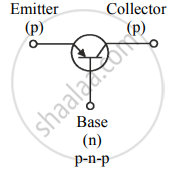
Figure (a)
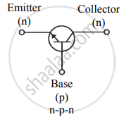
Figure (b)
The difference in the Emitter (E), the Base (b), and the Collector (C) are as follows:
- Emitter: It is a thick heavily doped layer. This supplies a large number of majority carriers for the current flow through the transistor
- Base: It is the thin, lightly doped central layer.
- Collector: It is a thick and moderately doped layer. Its area is larger than that of the emitter and the base. This layer collects a major portion of the majority of carriers supplied by the emitter. The collector also helps dissipation of any small amount of heat generated.
APPEARS IN
RELATED QUESTIONS
In a transistor amplifier, IC = 5.5 mA , IE = 5.6 mA. The current amplification factor β is ______
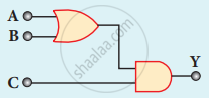
The output of the following circuit is 1 when the input ABC is
Give the Barkhausen conditions for sustained oscillations.
Explain the need for a feedback circuit in a transistor oscillator.
What is rectification?
In a common emitter amplifier, the input resistance is 1000 Ω, the peak value of Input signal voltage is 5 mV, and β = 60. The peak value of output current is
A transistor having α = 0.8 is connected in common emitter configuration. When the base current changes by 6 mA, then the change in collector current is ______.
If `alpha`-current gain of a transistor is 0.98. What is the value of `beta`- current gain of the transistor?
In an npn transistor, the base current is 100 µA and the collector current is 10 mA. The emitter current is ______.
ln switching circuit, transistor is in ON state and values of IC and IB are 4.2 mA and 5 µA respectively and RC= l k`Omega` and RB= 300 k`Omega`. If VBE = 0.5 V, find the value of VBB.
In a transistor in CE configuration, the ratio of power gain to voltage gain is ____________.
In switching circuit, transistor is in ON state, values of IE and lB are 10 mA and 0.8 mA respectively and RL is 2 k`Omega`. If VCE is 7.6 V, then VCC is ____________.
In a common emitter amplifier circuit using an n-p-n transistor, the phase difference between the input and the output voltages will be: ____________.
For a common emitter configuration, if 'α' and 'β' have their usual meanings, the correct relationship between 'α' and 'β' is ______.
In a silicon transistor, a change of 7.89 mA in the emitter current if produces a change of 7.8 mA in the collector current, then the base current must change by ____________.
In a transistor, the thickness of the base region ____________.
In transistor amplifier, base-emitter junction is forward biased and collector emitter junction is reverse biased. The current gain is ______.
In the case of transistor, the relation between current ratios αdc and βdc is ______.
A transistor is connected in C - E mode. If collector current is 72 × 10-5 A and α = 0.96, then base current will be ______.
In common emitter amplifier, a change of 0.2 mA in the base current causes a change of 5 mA in the collector current. If input resistance is 2K `Omega` and voltage gain is 75, the load resistance used in the circuit is ______.
The reverse bias in a junction diode is changed from 8V to 13V, then the value of the current changes from 40μA to 60μA. The resistance of junction diode will be ______.
The base current in common emitter mode of the transistor changes by 10 µA. If the current gain of the transistor is 50, then change in collector current is ______.
The collector current in a common-emitter transistor amplifier is 4 mA. When the base current is increased by 20 µA, the collector current increases to 6 mA. The current gain is ______.
In a CE amplifier, the current gain is 80 and the emitter current is 9 mA. The base current is ______.
Explain the output characteristics of common emitter configuration of n-p-n transistor.
Define β
For a common emitter transistor configuration the ratio of `I_c/I_E` = 0.96, then the current gain in this configuration is ______.
