Advertisements
Advertisements
प्रश्न
Draw the circuit symbol for NPN and PNP transistors. What is the difference in the Emitter, Base, and Collector regions of a transistor?
Advertisements
उत्तर
The circuit symbols of the two types of transistors:
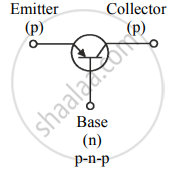
Figure (a)
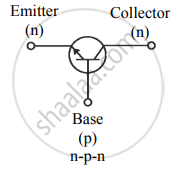
Figure (b)
The difference in the Emitter (E), the Base (b), and the Collector (C) are as follows:
- Emitter: It is a thick heavily doped layer. This supplies a large number of majority carriers for the current flow through the transistor
- Base: It is the thin, lightly doped central layer.
- Collector: It is a thick and moderately doped layer. Its area is larger than that of the emitter and the base. This layer collects a major portion of the majority of carriers supplied by the emitter. The collector also helps dissipation of any small amount of heat generated.
APPEARS IN
संबंधित प्रश्न
Why are the emitter, the base, and the collector of a BJT doped differently?
In a common-base connection, a certain transistor has an emitter current of 10mA and a collector current of 9.8 mA. Calculate the value of the base current.
With the help of a neat circuit diagram, explain the transistor as an amplifier?
Draw the circuit diagram to study the characteristic of the transistor in common emitter mode. Draw the input and output characteristics.
The light emitted in an LED is due to
Explain the current flow in an NPN transistor.
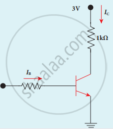
Assuming VCEsat = 0.2 V and β = 50, find the minimum base current (IB) required to drive the transistor given in the figure to saturation.
For a transistor, the current ratio 'βdc' is defined as the ratio of ______.
In the symbol for a transistor, the arrow head points in the direction of the ____________.
Least doped region in a transistor ____________.
In an npn transistor, the base current is 100 µA and the collector current is 10 mA. The emitter current is ______.
In an npn transistor, the collector current is 24 mA. If 80% of electrons reach collector, its base current in mA is ______.
ln switching circuit, transistor is in ON state and values of IC and IB are 4.2 mA and 5 µA respectively and RC= l k`Omega` and RB= 300 k`Omega`. If VBE = 0.5 V, find the value of VBB.
For a common emitter configuration, if 'α' and 'β' have their usual meanings, the correct relationship between 'α' and 'β' is ______.
In a transistor, a change of 8.0 mA in the emitter current produces a change of 7.8 mA in the collector current. Then change in the base current is ____________.
A pnp transistor is used in common-emitter mode. If a change of 40 µA in base current brings a change of 2 µA in collector current with 0.04 V in base-emitter voltage, then the input resistance is ____________.
In a transistor, doping level in base is increased slightly, the collector current and base current respectively ______.
In the common-emitter configuration of a transistor, the current gain is more than 1 because [lb, le, and lc are base, emitter, and collector currents respectively] ______
A conducting wire has length 'L1' and diameter 'd1'. After stretching the same wire length becomes 'L2' and diameter 'd2' The ratio of resistances before and after stretching is ______.
The reverse bias in a junction diode is changed from 8V to 13V, then the value of the current changes from 40μA to 60μA. The resistance of junction diode will be ______.
The transfer ratio of a transistor is 50. The input resistance of the transistor when used in the CE configuration is 1K Ω. The peak value for an AC input voltage of 0.01 V of collector current is ______.
How is a transistor biased for operating it as amplifier?
Explain the output characteristics of common emitter configuration of n-p-n transistor.
When an n-p-n junction transistor is used as an amplifier in common emitter mode, ______.
For a common emitter transistor configuration the ratio of `I_c/I_E` = 0.96, then the current gain in this configuration is ______.
In the case of constants ‘α’ and ‘β’ of a transistor ______.
