Advertisements
Advertisements
प्रश्न
With the help of a neat circuit diagram, explain the transistor as an amplifier?
Advertisements
उत्तर
Working of an amplifier:
- The circuit of an amplifier using an n-p-n transistor in CE configuration is shown in the figure.
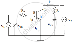
- When the input voltage Vin is not applied, applying the Kirchhoff’s law to the output loop, we can write, VCC = VCE + ICRL
- Similarly, for input loop,
VBB = VBE + IBRB - When the input AC signal is applied, Vin is not zero. Thus, the voltage drop across the input loop will now be,
VBB + Vin = VBE + IBRB + ΔIB (RB + ri) ....(1) - The AC signal applied adds the current of ΔIB to the original current flowing through the circuit. Therefore, the additional voltage drop in the input loop will be across resistor RB (= ΔIBRB) and across the input dynamic resistance of the transistor (= ΔIBri).
- From equation (1),
Vin = ΔIB (RB + ri)
As, RB is very small, we can consider,
Vin = ΔIBri - The changes in the base current IB cause changes in the collector current IC. This changes the voltage drop across the load resistance because VCC is constant. We can write,
ΔVCC = ΔVCE + RLIC = 0
∴ ΔVCE = -RLIC - The change in the output voltage ΔVCE is the output voltage Vo hence we can write,
Vo = ΔVCE = `beta`ACRLΔIB
APPEARS IN
संबंधित प्रश्न
In a BJT, the largest current flow occurs ______.
Why is the base of a transistor made thin and is lightly doped?
In a common-base connection, the emitter current is 6.28 mA and the collector current is 6.20 mA. Determine the common-base DC current gain.
Derive the relation between α and β.
In a common base configuration, the transistor has an emitter current of 10 mA and a collector current of 9.8 mA. The value of base current is ______
In a transistor amplifier, IC = 5.5 mA , IE = 5.6 mA. The current amplification factor β is ______
With the help of a neat diagram, explain the working of the npn transistor?
The light emitted in an LED is due to
Explain the current flow in an NPN transistor.
Explain the need for a feedback circuit in a transistor oscillator.
Transistor functions as a switch. Explain.
A common emitter amplifier is designed with n-p-n transistor (α = 0.99). The input impedance is 1 kΩ and the load is 10 kΩ. The voltage gain will be ______
In the symbol for a transistor, the arrow head points in the direction of the ____________.
In an npn transistor, the base current is 100 µA and the collector current is 10 mA. The emitter current is ______.
ln switching circuit, transistor is in ON state and values of IC and IB are 4.2 mA and 5 µA respectively and RC= l k`Omega` and RB= 300 k`Omega`. If VBE = 0.5 V, find the value of VBB.
A transistor when connected in common emitter mode has a ____________.
In common emitter mode of transistor, the d.c. current gain is 20, the emitter current is 7 mA. The collector current is ______.
In a p-n-p transistor circuit, the collector current is 10 mA. If 90% of the holes emitted from the emitter reach the collector, ______.
The current amplification factor for a transistor in its common emitter mode is 50. The current amplification factor in the common base mode of the transistor is ______.
Explain the working of the n-p-n transistor in a common base configuration.
The collector current in a common-emitter transistor amplifier is 4 mA. When the base current is increased by 20 µA, the collector current increases to 6 mA. The current gain is ______.
How is a transistor biased for operating it as amplifier?
In a CE amplifier, the current gain is 80 and the emitter current is 9 mA. The base current is ______.
When an n-p-n junction transistor is used as an amplifier in common emitter mode, ______.
For a common emitter transistor configuration the ratio of `I_c/I_E` = 0.96, then the current gain in this configuration is ______.
In the case of constants ‘α’ and ‘β’ of a transistor ______.
