Advertisements
Advertisements
Questions
Derive the relation between α and β.
Obtain the relation between the current gain αDC and βDC for a transistor.
Advertisements
Solution
In common emitter configuration, the emitter current is
IE = IB + lC ...(i)
Dividing the above equation by lC we get
`"I"_"E"/"I"_"C" = "I"_"B"/"I"_"C" + 1`
By definition of αDC and βDC
∴ `1/alpha_"DC" = 1/beta_"DC" + 1` ...(ii)
`1/alpha_"DC" = (beta_"DC" + 1)/beta_"DC"`
∴ `alpha_"DC" = beta_"DC"/(1 + beta_"DC")`
∴ `alpha_"DC" = beta/(1 + beta)` ...(iii)
Also, from equation (ii),
`1/alpha_"DC" - 1 = 1/beta_"DC"`
`(1 - alpha_"DC")/alpha_"DC" = 1/beta_"DC"`
∴ `beta_"DC" = alpha_"DC"/(1 - alpha_"dc")`
∴ `beta_"DC" = alpha/(1 - alpha)` ...(iv)
RELATED QUESTIONS
Why are the emitter, the base, and the collector of a BJT doped differently?
In a common base configuration, the transistor has an emitter current of 10 mA and a collector current of 9.8 mA. The value of base current is ______
For a transistor β =75 and IE = 7.5 mA. The value of α is ______
For a transistor IC = 15 mA, IB = 0.5 mA. What is the current amplification factor?
Draw the circuit symbol for NPN and PNP transistors. What is the difference in the Emitter, Base, and Collector regions of a transistor?
With the help of a neat diagram, explain the working of the npn transistor?
With the help of a neat circuit diagram, explain the transistor as an amplifier?
Draw the circuit diagram to study the characteristic of the transistor in common emitter mode. Draw the input and output characteristics.
The light emitted in an LED is due to
What is rectification?
Transistor functions as a switch. Explain.
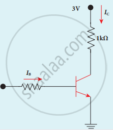
Assuming VCEsat = 0.2 V and β = 50, find the minimum base current (IB) required to drive the transistor given in the figure to saturation.
A common emitter amplifier is designed with n-p-n transistor (α = 0.99). The input impedance is 1 kΩ and the load is 10 kΩ. The voltage gain will be ______
A transistor having α = 0.8 is connected in common emitter configuration. When the base current changes by 6 mA, then the change in collector current is ______.
If l1, l2, l3 are the lengths of the emitter, base and collector of a transistor, then ____________.
For a transistor, the current ratio 'βdc' is defined as the ratio of ______.
In the study of transistor as an amplifier, the ratio of collector current to emitter current is 0.98 then the ratio of collector current to base current will be ______.
ln switching circuit, transistor is in ON state and values of IC and IB are 4.2 mA and 5 µA respectively and RC= l k`Omega` and RB= 300 k`Omega`. If VBE = 0.5 V, find the value of VBB.
In a common emitter amplifier circuit using an n-p-n transistor, the phase difference between the input and the output voltages will be: ____________.
In a transistor, a change of 8.0 mA in the emitter current produces a change of 7.8 mA in the collector current. Then change in the base current is ____________.
In transistor amplifier, base-emitter junction is forward biased and collector emitter junction is reverse biased. The current gain is ______.
For an ideal diode, the current in the following arrangement is ______.

A common emitter amplifier has a voltage gain of 50, an input impedance of 100Ω and an output impedance of 2000Ω. The power gain of the amplifier is ______.
The base current in common emitter mode of the transistor changes by 10 µA. If the current gain of the transistor is 50, then change in collector current is ______.
In a CE amplifier, the current gain is 80 and the emitter current is 9 mA. The base current is ______.
Define β
In a transistor (common emitter configuration) the ratio of power gain to voltage gain is (α and β are current ratios) ______.
