Advertisements
Advertisements
Question
Why is the base of a transistor made thin and is lightly doped?
Advertisements
Solution
The base of a transistor is lightly doped than the emitter and narrowed so that almost all electrons injected from the emitter (in a n-p-n transistor) diffuse right across the base to the collector junction without recombining with holes. In other words, the base width is kept smaller than the recombination distance. In addition, to improve emitter efficiency and common-base current gain α, the emitter is much more heavily doped than the base.
APPEARS IN
RELATED QUESTIONS
In a common base configuration, the transistor has an emitter current of 10 mA and a collector current of 9.8 mA. The value of base current is ______
Explain the need for a feedback circuit in a transistor oscillator.
Sketch the static characteristics of a common emitter transistor and bring out the essential features of input and output characteristics.
Describe the function of a transistor as an amplifier with the neat circuit diagram. Sketch the input and output wave forms.
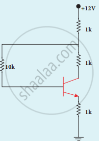
A transistor of α = 0.99 and VBE = 0.7 V is connected in the common-emitter configuration as shown in the figure. If the transistor is in the saturation region, find the value of collector current.
In the circuit shown in the figure, the BJT has a current gain (β) of 50. For an emitter-base voltage VEB = 600 mV, calculate the emitter-collector voltage VEC (in volts).
A common emitter amplifier is designed with n-p-n transistor (α = 0.99). The input impedance is 1 kΩ and the load is 10 kΩ. The voltage gain will be ______
If l1, l2, l3 are the lengths of the emitter, base and collector of a transistor, then ____________.
Ve, Vb, and Ve are emitter, base, and collector voltage respectively for npn transistor in CE mode. Amplifier works for the combination of biasing voltage equal to ______.
In an npn transistor, the collector current is 24 mA. If 80% of electrons reach collector, its base current in mA is ______.
ln switching circuit, transistor is in ON state and values of IC and IB are 4.2 mA and 5 µA respectively and RC= l k`Omega` and RB= 300 k`Omega`. If VBE = 0.5 V, find the value of VBB.
In switching circuit, transistor is in ON state, values of IE and lB are 10 mA and 0.8 mA respectively and RL is 2 k`Omega`. If VCE is 7.6 V, then VCC is ____________.
In a common emitter amplifier circuit using an n-p-n transistor, the phase difference between the input and the output voltages will be: ____________.
For a common emitter configuration, if 'α' and 'β' have their usual meanings, the correct relationship between 'α' and 'β' is ______.
A transistor when connected in common emitter mode has a ____________.
A pnp transistor is used in common-emitter mode. If a change of 40 µA in base current brings a change of 2 µA in collector current with 0.04 V in base-emitter voltage, then the input resistance is ____________.
The current gain `alpha` of a transistor is 0.95. The change in collector current corresponding to a change of 0.4 mA in the base current in a common emitter arrangement is ______.
For an ideal diode, the current in the following arrangement is ______.

In common emitter amplifier, a change of 0.2 mA in the base current causes a change of 5 mA in the collector current. If input resistance is 2K `Omega` and voltage gain is 75, the load resistance used in the circuit is ______.
A transistor is used as a common emitter amplifier with a load resistance 2 KΩ. The input resistance is 150 Ω. Base current is changed by 20 µA which results in a change in collector current by 1.5 mA. The voltage gain of the amplifier is ______.
In a p-n-p transistor circuit, the collector current is 10 mA. If 90% of the holes emitted from the emitter reach the collector, ______.
The current amplification factor for a transistor in its common emitter mode is 50. The current amplification factor in the common base mode of the transistor is ______.
In a CE amplifier, the current gain is 80 and the emitter current is 9 mA. The base current is ______.
Define peak value of alternating signal.
Explain the output characteristics of common emitter configuration of n-p-n transistor.
