Advertisements
Advertisements
प्रश्न
Why is the base of a transistor made thin and is lightly doped?
Advertisements
उत्तर
The base of a transistor is lightly doped than the emitter and narrowed so that almost all electrons injected from the emitter (in a n-p-n transistor) diffuse right across the base to the collector junction without recombining with holes. In other words, the base width is kept smaller than the recombination distance. In addition, to improve emitter efficiency and common-base current gain α, the emitter is much more heavily doped than the base.
APPEARS IN
संबंधित प्रश्न
In a common-base connection, the emitter current is 6.28 mA and the collector current is 6.20 mA. Determine the common-base DC current gain.
In a common base configuration, the transistor has an emitter current of 10 mA and a collector current of 9.8 mA. The value of base current is ______
Draw the circuit symbol of the PNP transistor.
With the help of a neat circuit diagram, explain the transistor as an amplifier?
Draw the circuit diagram to study the characteristic of the transistor in common emitter mode. Draw the input and output characteristics.
What is rectification?
Describe the function of a transistor as an amplifier with the neat circuit diagram. Sketch the input and output wave forms.
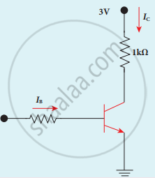
Assuming VCEsat = 0.2 V and β = 50, find the minimum base current (IB) required to drive the transistor given in the figure to saturation.
A transistor of α = 0.99 and VBE = 0.7 V is connected in the common-emitter configuration as shown in the figure. If the transistor is in the saturation region, find the value of collector current.
A transistor having α = 0.8 is connected in common emitter configuration. When the base current changes by 6 mA, then the change in collector current is ______.
In the symbol for a transistor, the arrow head points in the direction of the ____________.
In an npn transistor, the base current is 100 µA and the collector current is 10 mA. The emitter current is ______.
In an npn transistor, the collector current is 24 mA. If 80% of electrons reach collector, its base current in mA is ______.
In a transistor in CE configuration, the ratio of power gain to voltage gain is ____________.
In case of npn transistors, the collector current is always less than the emitter current because ______.
In a transistor, a change of 8.0 mA in the emitter current produces a change of 7.8 mA in the collector current. Then change in the base current is ____________.
The current gain `alpha` of a transistor is 0.95. The change in collector current corresponding to a change of 0.4 mA in the base current in a common emitter arrangement is ______.
In a transistor, doping level in base is increased slightly, the collector current and base current respectively ______.
In transistor amplifier, base-emitter junction is forward biased and collector emitter junction is reverse biased. The current gain is ______.
In a study of transistor as an amplifier, the ratio of collector current to emitter current is 0.98. The collector current is 3mA, then base current will be approximately ______.
In the common-emitter configuration of a transistor, the current gain is more than 1 because [lb, le, and lc are base, emitter, and collector currents respectively] ______
A conducting wire has length 'L1' and diameter 'd1'. After stretching the same wire length becomes 'L2' and diameter 'd2' The ratio of resistances before and after stretching is ______.
For a transistor, αdc and βdc are the current ratios, then the value of `(beta_"dc"-delta_"dc")/(alpha_"dc".beta_"dc")`
In a p-n-p transistor circuit, the collector current is 10 mA. If 90% of the holes emitted from the emitter reach the collector, ______.
The reverse bias in a junction diode is changed from 8V to 13V, then the value of the current changes from 40μA to 60μA. The resistance of junction diode will be ______.
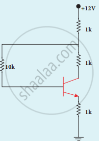
A common emitter amplifier circuit built using an n-p-n transistor is shown in the figure. Its DC current gain is 300, RC = 4 kΩ and VCC = 20 V. What is the minimum base current for VCE to reach saturation?

The collector current in a common-emitter transistor amplifier is 4 mA. When the base current is increased by 20 µA, the collector current increases to 6 mA. The current gain is ______.
In a CE amplifier, the current gain is 80 and the emitter current is 9 mA. The base current is ______.
Define peak value of alternating signal.
For a common emitter transistor configuration the ratio of `I_c/I_E` = 0.96, then the current gain in this configuration is ______.
