Advertisements
Advertisements
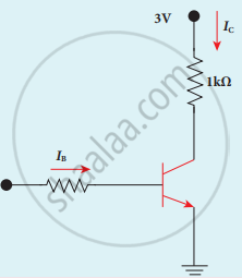
Question
For a transistor IC = 15 mA, IB = 0.5 mA. What is the current amplification factor?
Advertisements
Solution
Current amplification factor, β = `("I"_"c")/("I"_"B") = 15/0.5 = 30`
RELATED QUESTIONS
Why are the emitter, the base, and the collector of a BJT doped differently?
In a common-base connection, a certain transistor has an emitter current of 10mA and a collector current of 9.8 mA. Calculate the value of the base current.
In a common-base connection, the emitter current is 6.28 mA and the collector current is 6.20 mA. Determine the common-base DC current gain.
For a transistor β =75 and IE = 7.5 mA. The value of α is ______
The principle based on which a solar cell operates is ____________.
Give the Barkhausen conditions for sustained oscillations.
Explain the need for a feedback circuit in a transistor oscillator.
Sketch the static characteristics of a common emitter transistor and bring out the essential features of input and output characteristics.
Transistor functions as a switch. Explain.
Assuming VCEsat = 0.2 V and β = 50, find the minimum base current (IB) required to drive the transistor given in the figure to saturation.
A transistor has a voltage gain A. If the amount βA of its output is applied to the input of the transistor, then the transistor becomes oscillator, when ______.
If l1, l2, l3 are the lengths of the emitter, base and collector of a transistor, then ____________.
In the study of transistor as an amplifier, the ratio of collector current to emitter current is 0.98 then the ratio of collector current to base current will be ______.
In an npn transistor, the base current is 100 µA and the collector current is 10 mA. The emitter current is ______.
Which of the following regions of a transistors are, respectively, heavily dopped and lightly dopped?
In a common emitter amplifier circuit using an n-p-n transistor, the phase difference between the input and the output voltages will be: ____________.
In case of npn transistors, the collector current is always less than the emitter current because ______.
For a common emitter configuration, if 'α' and 'β' have their usual meanings, the correct relationship between 'α' and 'β' is ______.
A pnp transistor is used in common-emitter mode. If a change of 40 µA in base current brings a change of 2 µA in collector current with 0.04 V in base-emitter voltage, then the input resistance is ____________.
In a transistor, doping level in base is increased slightly, the collector current and base current respectively ______.
In transistor amplifier, base-emitter junction is forward biased and collector emitter junction is reverse biased. The current gain is ______.
A transistor is connected in C - E mode. If collector current is 72 × 10-5 A and α = 0.96, then base current will be ______.
A transistor having α = 0.8 is connected in a common emitter configuration. When the base current changes by 6 mA, the change in collector current is ______
A conducting wire has length 'L1' and diameter 'd1'. After stretching the same wire length becomes 'L2' and diameter 'd2' The ratio of resistances before and after stretching is ______.
The reverse bias in a junction diode is changed from 8V to 13V, then the value of the current changes from 40μA to 60μA. The resistance of junction diode will be ______.
The base current in common emitter mode of the transistor changes by 10 µA. If the current gain of the transistor is 50, then change in collector current is ______.
Explain the output characteristics of common emitter configuration of n-p-n transistor.
In a transistor (common emitter configuration) the ratio of power gain to voltage gain is (α and β are current ratios) ______.
