Advertisements
Advertisements
प्रश्न
For a transistor IC = 15 mA, IB = 0.5 mA. What is the current amplification factor?
Advertisements
उत्तर
Current amplification factor, β = `("I"_"c")/("I"_"B") = 15/0.5 = 30`
संबंधित प्रश्न
In a BJT, the largest current flow occurs ______.
In a common-base connection, a certain transistor has an emitter current of 10mA and a collector current of 9.8 mA. Calculate the value of the base current.
Derive the relation between α and β.
With the help of a neat diagram, explain the working of the npn transistor?
The principle based on which a solar cell operates is ____________.
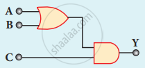
The output of the following circuit is 1 when the input ABC is
Explain the current flow in an NPN transistor.
What is rectification?
The condition to convert an amplified signal into an oscillating signal is ______
For a transistor, the current ratio 'βdc' is defined as the ratio of ______.
In the symbol for a transistor, the arrow head points in the direction of the ____________.
ln switching circuit, transistor is in ON state and values of IC and IB are 4.2 mA and 5 µA respectively and RC= l k`Omega` and RB= 300 k`Omega`. If VBE = 0.5 V, find the value of VBB.
Which of the following regions of a transistors are, respectively, heavily dopped and lightly dopped?
In case of npn transistors, the collector current is always less than the emitter current because ______.
A pnp transistor is used in common-emitter mode. If a change of 40 µA in base current brings a change of 2 µA in collector current with 0.04 V in base-emitter voltage, then the input resistance is ____________.
In a transistor, the thickness of the base region ____________.
In a transistor, doping level in base is increased slightly, the collector current and base current respectively ______.
In common emitter mode of transistor, the d.c. current gain is 20, the emitter current is 7 mA. The collector current is ______.
A change of 9.0 mA in the emitter current brings a change of 8.9 mA in the collector current. The value of current gain β will be ______.
For an ideal diode, the current in the following arrangement is ______.

A common emitter amplifier has a voltage gain of 50, an input impedance of 100Ω and an output impedance of 2000Ω. The power gain of the amplifier is ______.
The reverse bias in a junction diode is changed from 8V to 13V, then the value of the current changes from 40μA to 60μA. The resistance of junction diode will be ______.
The current amplification factor for a transistor in its common emitter mode is 50. The current amplification factor in the common base mode of the transistor is ______.
Explain the working of the n-p-n transistor in a common base configuration.
How is a transistor biased for operating it as amplifier?
Explain the output characteristics of common emitter configuration of n-p-n transistor.
When an n-p-n junction transistor is used as an amplifier in common emitter mode, ______.
In a transistor (common emitter configuration) the ratio of power gain to voltage gain is (α and β are current ratios) ______.
