Advertisements
Advertisements
Question
Describe the function of a transistor as an amplifier with the neat circuit diagram. Sketch the input and output wave forms.
Advertisements
Solution
i. Amplification is the process of increasing the signal strength (increase in the amplitude)
ii. NPN transistor is connected in CE configuration
iii. To start with, the Q point is fixed to get a maximum signal swing at the output.
iv. RC – to measure the output voltage
C1 allows only AC signals to pass,
Bypass capacitor CE provides a low resistance path
Coupling capacitor CC is used to couples the next stage amplifier.
Vs input source signal
IC = BIB `(∴ "B" = "I"_"C"/"I"_"B")`
VCE = VCC – ICRC

Transistor as an amplifier

Input and output waveforms showing 180° phase reversal.
Working of the amplifier:
a. Working of the amplifier:
- Input signal Vs increases the forward voltage across the emitter-base. IB increases. also increases IC also increases β times.
- This increases the voltage drop across Rc which decreases VCE.
- Therefore input signal in the positive direction produces an amplified signal in the negative direction at the output. Hence output signal is reversed by 180°.
b. During negative half cycle:
- Input signal Vs decreases the forwarded voltage across the emitter-base. As a result, IB decreases IC increases.
- Increase in IC decreases potential drop across Rc and increases VCE.
- Input signal in negative direction produces an amplified signal in the positive direction at the output.
- Therefore 180° phase reversal is observed during the negative half signal.
APPEARS IN
RELATED QUESTIONS
In a transistor amplifier, IC = 5.5 mA , IE = 5.6 mA. The current amplification factor β is ______
Draw the circuit symbol for NPN and PNP transistors. What is the difference in the Emitter, Base, and Collector regions of a transistor?
With the help of a neat diagram, explain the working of the npn transistor?
Draw the circuit diagram to study the characteristic of the transistor in common emitter mode. Draw the input and output characteristics.
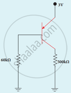
In the circuit shown in the figure, the BJT has a current gain (β) of 50. For an emitter-base voltage VEB = 600 mV, calculate the emitter-collector voltage VEC (in volts).
A transistor has a voltage gain A. If the amount βA of its output is applied to the input of the transistor, then the transistor becomes oscillator, when ______.
For a transistor, the current ratio 'βdc' is defined as the ratio of ______.
In the symbol for a transistor, the arrow head points in the direction of the ____________.
A change of 9.0 mA in the emitter current brings a change of 8.9 mA in the collector current. The value of current gain β will be ______.
For a common emitter transistor configuration the ratio of `I_c/I_E` = 0.96, then the current gain in this configuration is ______.
