Advertisements
Advertisements
प्रश्न
Draw the circuit symbol of the PNP transistor.
Advertisements
उत्तर
The circuit symbol of the p-n-p transistor

APPEARS IN
संबंधित प्रश्न
In a BJT, the largest current flow occurs ______.
Why are the emitter, the base, and the collector of a BJT doped differently?
Derive the relation between α and β.
For a transistor IC = 15 mA, IB = 0.5 mA. What is the current amplification factor?
With the help of a neat circuit diagram, explain the transistor as an amplifier?
The principle based on which a solar cell operates is ____________.
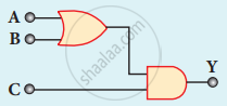
The output of the following circuit is 1 when the input ABC is
Describe the function of a transistor as an amplifier with the neat circuit diagram. Sketch the input and output wave forms.
A common emitter amplifier is designed with n-p-n transistor (α = 0.99). The input impedance is 1 kΩ and the load is 10 kΩ. The voltage gain will be ______
In an npn transistor, the base current is 100 µA and the collector current is 10 mA. The emitter current is ______.
In an npn transistor, the collector current is 24 mA. If 80% of electrons reach collector, its base current in mA is ______.
ln switching circuit, transistor is in ON state and values of IC and IB are 4.2 mA and 5 µA respectively and RC= l k`Omega` and RB= 300 k`Omega`. If VBE = 0.5 V, find the value of VBB.
In a common emitter amplifier circuit using an n-p-n transistor, the phase difference between the input and the output voltages will be: ____________.
For a common emitter configuration, if 'α' and 'β' have their usual meanings, the correct relationship between 'α' and 'β' is ______.
A transistor when connected in common emitter mode has a ____________.
In a transistor, the thickness of the base region ____________.
In a transistor, doping level in base is increased slightly, the collector current and base current respectively ______.
A transistor having α = 0.8 is connected in a common emitter configuration. When the base current changes by 6 mA, the change in collector current is ______
In the common-emitter configuration of a transistor, the current gain is more than 1 because [lb, le, and lc are base, emitter, and collector currents respectively] ______
A transistor is used as a common emitter amplifier with a load resistance 2 KΩ. The input resistance is 150 Ω. Base current is changed by 20 µA which results in a change in collector current by 1.5 mA. The voltage gain of the amplifier is ______.
The reverse bias in a junction diode is changed from 8V to 13V, then the value of the current changes from 40μA to 60μA. The resistance of junction diode will be ______.
A common emitter amplifier circuit built using an n-p-n transistor is shown in the figure. Its DC current gain is 300, RC = 4 kΩ and VCC = 20 V. What is the minimum base current for VCE to reach saturation?

How is a transistor biased for operating it as amplifier?
When an n-p-n junction transistor is used as an amplifier in common emitter mode, ______.
