Advertisements
Advertisements
प्रश्न
In a BJT, the largest current flow occurs ______.
विकल्प
In the emitter
In the collector
In the base
Through CB junction
Advertisements
उत्तर
In a BJT, the largest current flow occurs in the emitter.
Explanation:
Emitter is a thick, heavily doped layer. This supplies a large number of majority carriers for the current flow through the transistor
APPEARS IN
संबंधित प्रश्न
The common-base DC current gain of a transistor is 0.967. If the emitter current is 10mA. What is the value of base current?
Draw the circuit symbol for NPN and PNP transistors. What is the difference in the Emitter, Base, and Collector regions of a transistor?
With the help of a neat circuit diagram, explain the transistor as an amplifier?
Draw the circuit diagram to study the characteristic of the transistor in common emitter mode. Draw the input and output characteristics.
The light emitted in an LED is due to
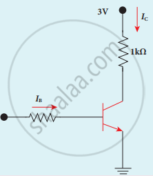
Assuming VCEsat = 0.2 V and β = 50, find the minimum base current (IB) required to drive the transistor given in the figure to saturation.
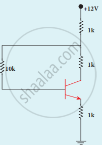
A transistor of α = 0.99 and VBE = 0.7 V is connected in the common-emitter configuration as shown in the figure. If the transistor is in the saturation region, find the value of collector current.
For a transistor, the current ratio 'βdc' is defined as the ratio of ______.
In the symbol for a transistor, the arrow head points in the direction of the ____________.
In the study of transistor as an amplifier, the ratio of collector current to emitter current is 0.98 then the ratio of collector current to base current will be ______.
In switching circuit, transistor is in ON state. Values of IC and IB are 5.2 mA and 10 µA respectively and value of RC is 1 k`Omega`. If Vcc is at 5.5 V, then VCE is ______.
Ve, Vb, and Ve are emitter, base, and collector voltage respectively for npn transistor in CE mode. Amplifier works for the combination of biasing voltage equal to ______.
If `alpha`-current gain of a transistor is 0.98. What is the value of `beta`- current gain of the transistor?
In an npn transistor, the base current is 100 µA and the collector current is 10 mA. The emitter current is ______.
Which of the following regions of a transistors are, respectively, heavily dopped and lightly dopped?
In a transistor, a change of 8.0 mA in the emitter current produces a change of 7.8 mA in the collector current. Then change in the base current is ____________.
In a transistor, the thickness of the base region ____________.
In the case of transistor, the relation between current ratios αdc and βdc is ______.
In common emitter mode of transistor, the d.c. current gain is 20, the emitter current is 7 mA. The collector current is ______.
A transistor is connected in C - E mode. If collector current is 72 × 10-5 A and α = 0.96, then base current will be ______.
In common emitter amplifier, a change of 0.2 mA in the base current causes a change of 5 mA in the collector current. If input resistance is 2K `Omega` and voltage gain is 75, the load resistance used in the circuit is ______.
For a transistor, αdc and βdc are the current ratios, then the value of `(beta_"dc"-delta_"dc")/(alpha_"dc".beta_"dc")`
In a p-n-p transistor circuit, the collector current is 10 mA. If 90% of the holes emitted from the emitter reach the collector, ______.
A common emitter amplifier circuit built using an n-p-n transistor is shown in the figure. Its DC current gain is 300, RC = 4 kΩ and VCC = 20 V. What is the minimum base current for VCE to reach saturation?

The base current in common emitter mode of the transistor changes by 10 µA. If the current gain of the transistor is 50, then change in collector current is ______.
Define β
In the case of constants ‘α’ and ‘β’ of a transistor ______.
