Advertisements
Advertisements
प्रश्न
A student wants to use two p-n junction diodes to convert alternating current into direct current. Draw the labelled circuit diagram she would use and explain how it works.
Advertisements
उत्तर
The student will use a full wave rectifier.
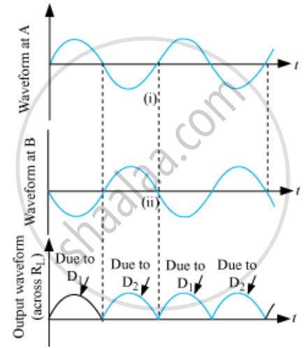
Two diodes are used to give rectified O/P corresponding to both positive as well as negative half cycles.
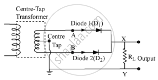
When the voltage at A with respect to the centre tap is positive, and the voltage at B is negative. Then, D1 is forward biased and D2 is reversed biased. Hence, D1 conducts and D2 does not.
When the voltage of A becomes negative, then B becomes + ve. Therefore, D1 does not conduct and D2 conducts. Hence, we obtain output voltage during both the positive as well as negative half of cycle.
APPEARS IN
संबंधित प्रश्न
How is a zener diode fabricated so as to make it a special purpose diode? Draw I-V characteristics of zener diode and explain the significance of breakdown voltage.
Explain briefly, with the help of a circuit diagram, how a p-n junction diode works as a half wave rectifier.
The diffusion current in a p-n junction is
Diffusion current in a p-n junction is greater than the drift current in magnitude
In a p-n junction,
(a) new holes and conduction electrons are produced continuously throughout the material
(b) new holes and conduction electrons are produced continuously throughout the material except in the depletion region
(c) holes and conduction electrons recombine continuously throughout the material
(d) holes and conduction electrons recombine continuously throughout the material except in the depletion region.
A semiconducting device is connected in a series circuit with a battery and a resistance. A current is found to pass through the circuit. If the polarity of the battery is reversed, the current drops to almost zero. the device may be
(a) an intrinsic semiconductor
(b) a p-type semiconductor
(c) an n-type semiconductor
(d) a p-n junction
When a p-n junction is reverse-biased, the current becomes almost constant at 25 µA. When it is forward-biased at 200 mV, a current of 75 µA is obtained. Find the magnitude of diffusion current when the diode is
(a) unbiased,
(b) reverse-biased at 200 mV and
(c) forward-biased at 200 mV.
Draw the current-voltage characteristics for the device show in figure between the terminals A and B.

(Assume that the resistance of each diode is zero in forward bias and is infinity in reverse bias.)
An AC source is connected to a diode and a resistor in series. Is the current thorough the resistor AC or DC?
Choose the correct option.
Current through a reverse-biased p-n junction increases abruptly at:
Answer in detail.
Discuss the effect of external voltage on the width of depletion region of a p-n junction.
