Advertisements
Advertisements
प्रश्न
The output of NOR gate is high, when _______.
पर्याय
all inputs are high
all inputs are low
only one of its inputs is high
only one of its inputs is low
Advertisements
उत्तर
all inputs are low
APPEARS IN
संबंधित प्रश्न
Which logic gate corresponds to the truth table given below?
|
A |
B |
Y |
|
0 |
0 |
I |
|
0 |
1 |
0 |
|
1 |
0 |
0 |
|
1 |
1 |
0 |
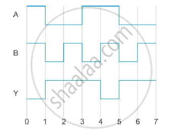
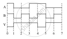
The following figure shows the input waveforms (A, B) and the output waveform (Y) of a gate. Identify the gate, write its truth table and draw its logic symbol.
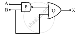
Identify the logic gates marked 'P' and 'Q' in the given circuit. Write the truth table for the combination.
You are given the two circuits as shown in following figure. Show that circuit
- acts as OR gate while the circuit
- acts as AND gate.
(a)
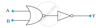
(b)
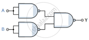
Write the truth table for a NAND gate connected as given in the following figure.
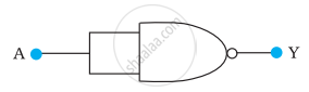
Hence identify the exact logic operation carried out by this circuit
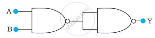
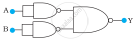
You are given two circuits as shown in following figure, which consist of NAND gates. Identify the logic operation carried out by the two circuits.
(a)
(b)
The following figure shows the input waveforms (A, B) and the output waveform (Y) of a gate. Identify the gate, write its truth table and draw its logic symbol.
What will be the values of input A and B for the Boolean expression `overline ((A +B) .(A*B)) =1?`
The output of an OR gate is connected to both the inputs of a NAND gate Draw the logic circuit of this combinaion of getes and write its truth table.
Let \[X = A \overline{ BC} + B\overline{ CA} + C\overline{AB } .\] Evaluate X for A = 1, B = 0, C = 1.
Let \[X = A \overline{ BC} + B\overline{ CA} + C\overline{AB } .\] Evaluate X for A = B = C = 1.
The amplification factor of a triode operating in the linear region depends strongly on ____________ .
Draw the truth table of a NOR gate.
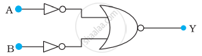
The outputs of two NOT gates are fed to a NOR gate. Draw the logic circuit of the combination of gates. Write its truth table. Identify the gate equivalent to this circuit.
You are given a circuit as shown in the figure, which consists of the NAND gate. Identify the logic operation carried out by the two. Write the truth table. Identify the gates equivalent to the tow circuit.
NAND and NOR gates are called universal gates primarily because they ______.
An oscillator is nothing but an amplifier with
A CE amplifier has a voltage gain 50, an input impedance of 1000 ohm 1 and an output impedance of 200 ohm. The power gain of the amplifier will be
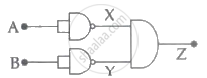
The truth table for the following logic circuit is:
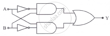
Truth table for the given circuit (Figure) is ______.
Two car garages have a common gate which needs to open automatically when a car enters either of the garages or cars enter both. Devise a circuit that resembles this situation using diodes for this situation.
Identify the logic operation carried out by the given circuit:
The given figure shows the waveforms for two inputs A and B and that for the output Y of a logic circuit. The logic circuit is ______.

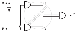
The output (Y) of the given logic implementation is similar to the output of an/a ______ gate.