मराठी
कर्नाटक बोर्ड पी.यू.सी.पीयूसी विज्ञान 2nd PUC Class 12

Write the truth table for circuit given in figure below consisting of NOR gates and identify the logic operation (OR, AND, NOT) which this circuit is performing. - Physics

Advertisements
Advertisements

प्रश्न

Write the truth table for circuit given in figure below consisting of NOR gates and identify the logic operation (OR, AND, NOT) which this circuit is performing.

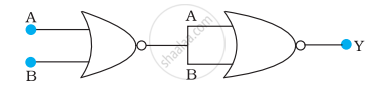
(Hint: A = 0, B = 1 then A and B inputs of second NOR gate will be 0 and hence Y=1. Similarly work out the values of Y for other combinations of A and B. Compare with the truth table of OR, AND, NOT gates and find the correct one.)

संख्यात्मक
Advertisements

उत्तर

A and B are the inputs of the given circuit. The output of the first NOR gate is `bar(A +B)`. It can be observed from the following figure that the inputs of the second NOR gate become the out put of the first one.

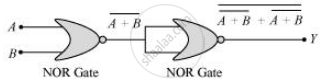
Hence, the output of the combination is given as:

`Y = bar(bar("A+B") + bar("A+B")) = bar(bar("A").bar("B")) + bar(bar"A".bar"B")`

`= bar(bar"A".bar"B") = bar(bar"A") + bar(bar"B") = "A + B"`

The truth table for this operation is given as:

B Y (=A + B)
0 0 0
0 1 1
1 0 1
1 1 1

This is the truth table of an OR gate. Hence, this circuit functions as an OR gate.

shaalaa.com
  या प्रश्नात किंवा उत्तरात काही त्रुटी आहे का?

व्हिडिओ ट्यूटोरियलVIEW ALL [3]

संबंधित प्रश्‍न

The following figure shows the input waveforms (A, B) and the output waveform (Y) of a gate. Identify the gate, write its truth table and draw its logic symbol.


Identify the logic gates marked 'P' and 'Q' in the given circuit. Write the truth table for the combination.


Write the truth table for the circuits given in following figure consisting of NOR gates only. Identify the logic operations (OR, AND, NOT) performed by the two circuits.

(a)

(b)


Draw the schematic symbols for AND, OR, NOT and NAND gate


You are given a circuit below. Write its truth table. Hence, identify the logic operation carried out by this circuit. Draw the logic symbol of the gate it corresponds to.


The following figure shows the input waveforms (A, B) and the output waveform (Y) of a gate. Identify the gate, write its truth table and draw its logic symbol.


Let  \[X = A \overline{ BC} + B\overline{ CA} + C\overline{AB } .\]   Evaluate X for A = 1, B = 0, C = 1. 


The amplification factor of a triode operating in the linear region depends strongly on ____________ .


Show the variation of voltage with time, for a digital signal.


Draw the truth table of a NOR gate.


With the help of a diagram, show how you can use several NAND gates to obtain an OR gate.

Useful Constants and Relations :

1. Speed of Light in Vacuum      (c) = 3.00 x 10⁸ m/s
2. Charge of a proton (e) = 1.60 x 10⁻¹⁹C
3. Planck's Constant (h) = 6.6 x 10⁻³⁴ Js
4. Permeability of vacuum 0) = 4π x 10-7 Hm-1
5. Electron Volt (1eV ) = 1.6 x 10 
6. Unified Atomic Mass Unit (1u) = 931 MeV
  (π) = 3.14
  ( ln 2 ) = 0.693

A radar is sending out pules of 1 micro second duration at interval of 100 micro-second. The range of the radar is


In potential barrier development in a junction diode opposes


For the given circuit, the input digital signals are applied at the terminals A, B and C. What would be the output at the terminal y?


How would you set up a circuit to obtain NOT gate using a transistor?


Write the truth table for the circuit shown in figure. Name the gate that the circuit resembles.


An X-OR gate has following truth table:

A B Y
0 0 0
0 1 1
1 0 1
1 1 0

It is represented by following logic relation `Y = barA.B + A.barB`. Build this gate using AND, OR and NOT gates.


In the logic circuit shown in the figure, if input A and B are 0 to 1 respectively, the output at Y would be 'x'. The value of x is ______.


Share
Notifications

Englishहिंदीमराठी


      Forgot password?
Use app×