Advertisements
Advertisements
प्रश्न
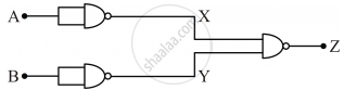
You are given a circuit below. Write its truth table. Hence, identify the logic operation carried out by this circuit. Draw the logic symbol of the gate it corresponds to.

Advertisements
उत्तर

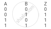
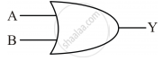
Hence, the gate is an OR gate.
The output is 1 when either of the input or both the inputs are 1.
Symbol:

APPEARS IN
संबंधित प्रश्न
Give the truth table and circuit symbol for NAND gate
Design a logical circuit using AND, OR and NOT gates to evaluate \[A \overline { BC } + B \overline{ CA }\] .
Show that \[AB + \overline {AB }\] is always 1.
Draw the truth table of a NOR gate.
The outputs of two NOT gates are fed to a NOR gate. Draw the logic circuit of the combination of gates. Write its truth table. Identify the gate equivalent to this circuit.
NAND and NOR gates are called universal gates primarily because they ______.
In potential barrier development in a junction diode opposes
Write the truth table for the circuit shown in figure. Name the gate that the circuit resembles.

In the logic circuit shown in the figure, if input A and B are 0 to 1 respectively, the output at Y would be 'x'. The value of x is ______.

A logic gate circuit has two inputs A and B and output Y. The voltage waveforms of A, B and Y are shown below.

The logic gate circuit is ______.
