Advertisements
Advertisements
प्रश्न
Write the truth table for a NAND gate connected as given in the following figure.

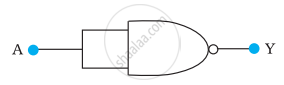
Hence identify the exact logic operation carried out by this circuit
Advertisements
उत्तर
A acts as the two inputs of the NAND gate and Y is the output, as shown in the following figure.

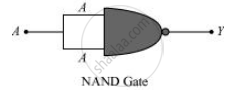
Hence, the output can be written as:
`Y = bar("A"."A") = bar"A" + bar"A" = bar"A"` ...(i)
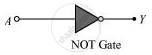
The truth table for equation (i) can be drawn as:
| A | Y`(=bar"A")` |
| 0 | 1 |
| 1 | 0 |
This circuit functions as a NOT gate. The symbol for this logic circuit is shown as:

संबंधित प्रश्न
You are given the two circuits as shown in following figure. Show that circuit
- acts as OR gate while the circuit
- acts as AND gate.
(a)

(b)

Write the truth table for circuit given in figure below consisting of NOR gates and identify the logic operation (OR, AND, NOT) which this circuit is performing.

(Hint: A = 0, B = 1 then A and B inputs of second NOR gate will be 0 and hence Y=1. Similarly work out the values of Y for other combinations of A and B. Compare with the truth table of OR, AND, NOT gates and find the correct one.)
Draw the schematic symbols for AND, OR, NOT and NAND gate
You are given a circuit below. Write its truth table. Hence, identify the logic operation carried out by this circuit. Draw the logic symbol of the gate it corresponds to.

Name the logic gate which generated high output when at least one input is high.
An AND gate can be prepared by repetitive use of
(a) NOT gate
(b) OR gate
(c) NAND gate
(d) NOR gate.
Let \[X = A \overline{ BC} + B\overline{ CA} + C\overline{AB } .\] Evaluate X for A = 1, B = 0, C = 1.
Show that \[AB + \overline {AB }\] is always 1.
The amplification factor of a triode operating in the linear region depends strongly on ____________ .
Show the variation of voltage with time, for a digital signal.
Draw a diagram to show how NAND gates can be combined to obtain an OR gate. (Truth table is not, required)
Useful Constants and Relations:
| 1. | Charge of a proton | (e) | =1.6 × 10⁻¹⁹C |
| 2. | Planck's constant | (h) | = 6·6 × 10-34 Js |
| 3. | Mass of an electron | (m) | = 9·1× 10-31 kg |
| 4. | Permittivity of vacuum | (∈0) | =8 · 85 × 10-12 Fm-1 |
| 5. | `(1/(4pi∈_0))` | =9 ×10⁹ mF-1 | |
| 6. | Permeability of vacuum | (μ0) | = 4π × 10-7 Hm-1 |
| 7. | `((mu_0)/(4pi))` | =1 × 10⁻⁷ Hm-1 | |
| 8. | Speed of light in vacuum | (c) | = 3× 10⁸ ms-1 |
| 9. | Unified atomic mass unit | (u) |
= 931 MeV |
| 10. | Electron volt | (leV) | = 1.6 × 10⁻¹⁹ J |
With the help of a diagram, show how you can use several NAND gates to obtain an OR gate.
Useful Constants and Relations :
| 1. Speed of Light in Vacuum | (c) = 3.00 x 10⁸ m/s |
| 2. Charge of a proton | (e) = 1.60 x 10⁻¹⁹C |
| 3. Planck's Constant | (h) = 6.6 x 10⁻³⁴ Js |
| 4. Permeability of vacuum | (μ0) = 4π x 10-7 Hm-1 |
| 5. Electron Volt | (1eV ) = 1.6 x 10 |
| 6. Unified Atomic Mass Unit | (1u) = 931 MeV |
| (π) = 3.14 | |
| ( ln 2 ) = 0.693 |
NAND and NOR gates are called universal gates primarily because they ______.
A radar is sending out pules of 1 micro second duration at interval of 100 micro-second. The range of the radar is
An oscillator is nothing but an amplifier with
An X-OR gate has following truth table:
| A | B | Y |
| 0 | 0 | 0 |
| 0 | 1 | 1 |
| 1 | 0 | 1 |
| 1 | 1 | 0 |
It is represented by following logic relation `Y = barA.B + A.barB`. Build this gate using AND, OR and NOT gates.
The output (Y) of the given logic implementation is similar to the output of an/a ______ gate.

