Advertisements
Advertisements
प्रश्न
You are given the two circuits as shown in following figure. Show that circuit
- acts as OR gate while the circuit
- acts as AND gate.
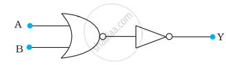
(a)
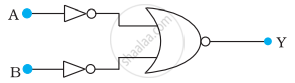
(b)
Advertisements
उत्तर
(a) A and B are the inputs and Y is the output of the given circuit. The left half of the given figure acts as the NOR Gate, while the right half acts as the NOT Gate. This is shown in the following figure.
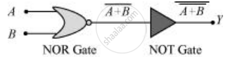
Hence, the output of the NOR Gate = `bar("A+B")`
This will be the input for the NOT Gate. Its output will be `bar(bar ("A + B"))` = A + B
∴ Y = A + B
Hence, this circuit functions as an OR Gate.
(b) A and B are the inputs and Y is the output of the given circuit. It can be observed from the following figure that the inputs of the right half NOR Gate are the outputs of the two NOT Gates
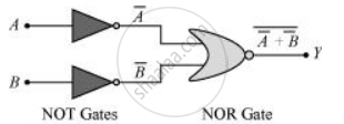
Hence, the output of the given circuit can be written as:
`Y = bar(bar"A" + bar"B")` = `bar(bar("A")). bar(bar"B")` = A.B
Hence, this circuit functions as an AND Gate.
