Advertisements
Advertisements
In what way is diffraction from each slit related to the interference pattern in a double-slit experiment?
Concept: Diffraction of Light >> The Single Slit
Draw the intensity pattern for single slit diffraction.
Concept: Diffraction of Light >> Seeing the Single Slit Diffraction Pattern
Draw the intensity pattern for double slit interference.
Concept: Diffraction of Light >> Seeing the Single Slit Diffraction Pattern
State differences between interference and diffraction patterns.
Concept: Diffraction of Light >> Seeing the Single Slit Diffraction Pattern
Use Huygens' principle to verify the laws of refraction.
Concept: Huygens Principle
Write three characteristic features to distinguish between the interference fringes in Young's double slit experiment and the diffraction pattern obtained due to a narrow single slit.
Concept: Interference of Light Waves and Young’s Experiment
In Young's double slit experiment, derive the condition for
(i) constructive interference and
(ii) destructive interference at a point on the screen.
Concept: Interference of Light Waves and Young’s Experiment
A beam of light consisting of two wavelengths, 800 nm and 600 nm is used to obtain the interference fringes in a Young's double slit experiment on a screen placed 1 · 4 m away. If the two slits are separated by 0·28 mm, calculate the least distance from the central bright maximum where the bright fringes of the two wavelengths coincide.
Concept: Interference of Light Waves and Young’s Experiment
How does an unpolarized light incident on a polaroid get polarized? Describe briefly, with the help of a necessary diagram, the polarization of light by reflection from a transparent medium.
Concept: Interference of Light Waves and Young’s Experiment
Two polaroids ‘A’ and ‘B’ are kept in crossed position. How should a third polaroid ‘C’ be placed between them so that the intensity of polarized light transmitted by polaroid B reduces to 1/8th of the intensity of unpolarized light incident on A?
Concept: Interference of Light Waves and Young’s Experiment
What is the effect on the interference fringes to a Young’s double slit experiment when
(i) the separation between the two slits is decreased?
(ii) the width of a source slit is increased?
(iii) the monochromatic source is replaced by a source of white light?
Justify your answer in each case.
Concept: Interference of Light Waves and Young’s Experiment
The intensity at the central maxima in Young’s double slit experimental set-up is I0. Show that the intensity at a point where the path difference is λ/3 is I0/4.
Concept: Interference of Light Waves and Young’s Experiment
Write the conditions on path difference under which constructive interference occurs in Young’s double-slit experiment.
Concept: Interference of Light Waves and Young’s Experiment
In a single slit diffraction experiment, the width of the slit is increased. How will the
- size and
- intensity
of central bright band be affected? Justify your answer.
Concept: Diffraction of Light >> The Single Slit
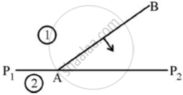
A plane wave front AB propagating from denser medium (1) into a rarer medium (2) is incident on the surface P1P2 separating the two media as shown in fig.
Using Huygen’s principle, draw the secondary wavelets and obtain the refracted wave front in the diagram.
Concept: Huygens Principle
In Young's double slit experiment using light of wavelength 600 nm, the slit separation is 0.8 mm and the screen is kept 1.6 m from the plane of the slits. Calculate
- the fringe width
- the distance of (a) third minimum and (b) fifth maximum, from the central maximum.
Concept: Interference of Light Waves and Young’s Experiment
According to Huygens’s principle, the amplitude of secondary wavelets is ______.
Concept: Huygens Principle
Write three characteristic features in photoelectric effect that cannot be explained on the basis of wave theory of light, but can be explained only using Einstein's equation.
Concept: Photoelectric Effect - Hertz’s Observations
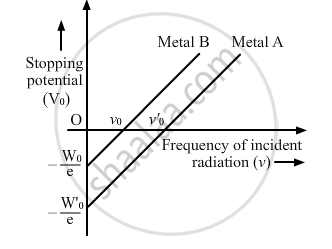
The graph shows the variation of stopping potential with frequency of incident radiation for two photosensitive metals A and B. Which one of the two has higher value of work-function? Justify your answer.
Concept: Photoelectric Effect - Hertz’s Observations
How does one explain the emission of electrons from a photosensitive surface with the help of Einstein's photoelectric equation?
Concept: Electron Emission
