Advertisements
Advertisements
प्रश्न
The width of depletion region of p-n junction diode is _______.
(A) 0.5 nm to 1 nm
(B) 5 nm to 10 nm
(C) 50 nm to 500 nm
(D) 500 nm to 1000 nm
Advertisements
उत्तर
500 nm to 1000 nm
APPEARS IN
संबंधित प्रश्न
With the help of a neat circuit diagram, explain the working of a photodiode.
How is a Zener diode fabricated?
If a small voltage is applied to a p-n junction diode, how will the barrier potential be affected when it is (i) forward biased
If a small voltage is applied to a p-n junction diode, how will the barrier potential be affected when it is(ii) reveres biased?
With what considerations in view, a photodiode is fabricated? State its working with the help of a suitable diagram.
Even though the current in the forward bias is known to be more than in the reverse bias, yet the photodiode works in reverse bias. What is the reason?
Using the necessary circuit diagrams, show how the V-I characteristics of a p-n junction are obtained in
Forward biasing
How are these characteristics made use of in rectification?
State its any ‘two’ uses of photodiode.
Describe, with the help of a circuit diagram, the working of a photodiode.
Sunil and his parents were travelling to their village in their car. On the way his mother noticed some grey coloured panels installed on the roof of a low building. She enquired from Sunil what those panels were and Sunil told his mother that those were solar panels.
(a) What were the values displayed by Sunil and his mother? State one value for each.
(b) In what way would the use of solar panels prove to be very useful?
(c) Name the semiconductor device used in solar panels. Briefly explain with the help of a diagram, how this device works
Write briefly the important processes that occur during the formation of p−n junction. With the help of necessary diagrams, explain the term 'barrier potential'.
Briefly explain its working. Draw its V - I characteristics for two different intensities of illumination ?
The current in the forward bias is known to be more (~mA) than the current in the reverse bias (~μA). What is the reason, then, to operate the photodiode in reverse bias?
Draw the circuit diagram of a full wave rectifier using p-n junction diode.
Explain its working and show the output, input waveforms.
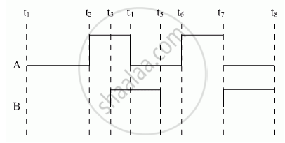
Show the output waveforms (Y) for the following inputs A and B of (i) OR gate (ii) NAND gate ?
Describe briefly, with the help of a diagram, the role of the two important processes involved in the formation of a p-n junction.
How does a light emitting diode (LED) work? Give two advantages of LED’s over the conventional incandescent lamps.
What happens to the width of depletion player of a p-n junction when it is (i) forward biased, (ii) reverse biased?
Draw the circuit diagram of an illuminated photodiode in reverse bias. How is photodiode used to measure light intensity?
An ideal diode should pass a current freely in one direction and should stop it completely in the opposite direction. Which is closer to ideal-vacuum diode or a p-njunction diode?
The plate resistance of a triode is 8 kΩ and the transconductance is 2.5 millimho. (a) If the plate voltage is increased by 48 V and the grid voltage is kept constant, what will be the increase in the plate current? (b) With plate voltage kept constant at this increased value, by how much should the grid voltage be decreased in order to bring the plate current back to its initial value?
Draw the circuit arrangement for studying the V-I characteristics of a p-n junction diode in reverse bias. Plot the V-I characteristics in this case.
Write the important considerations which are to be taken into account while fabricating a p-n junction diode to be used as a Light Emitting Diode (LED). What should be the order of band gap of an LED, if it is required to emit light in the visible range? Draw a circuit diagram and explain its action.
The wavelength and intensity of light emitted by a LED depend upon ______.
What is a solar cell?
Draw solar cell V-I characteristics.
With reference to Semiconductor Physics,
Name the process that causes depletion region in a p-n junction.
What is the magnitude of the potential barrier across a Ge p-n junction?
Name the device which converts the change in intensity of illumination to change in electric current flowing through it. Plot I-V characteristics of this device for different intensities. State any two applications of this device.
Pressure P varies as P = `alpha/beta "exp" (- (alpha x)/"k"_"BT")`, where x denotes the distance, kB is the Boltzmann's constant, T is the absolute temperature and α and β are constant. The dimension of β is ______.
A p-n photodiode is fabricated from a semiconductor with a band gap of 2.5 eV. lt can detect a signal of wavelength ______.
For LED's to emit light in visible region of electromagnetic light, it should have energy band gap in the range of:
Which one of the following is not the advantage of LED?
In Figure, assuming the diodes to be ideal ______.

If the resistance R1 is increased (Figure), how will the readings of the ammeter and voltmeter change?

Draw the circuit diagram of an illuminated photodiode and its I-V characteristics.
How can a photodiode be used to measure light intensity?
The value of power dissipated across the Zener diode (Vz = 15 V) connected in the circuit as shown in the figure is x × 10–1 watt. The value of x, to the nearest integer, is ______.

What energy conversion takes place in a solar cell?
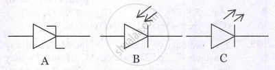
Identify the special purpose diodes 'A', 'B' and 'C' from the given symbols.
Select the wrong statement in the case of LED.
Consider the following statements A and B and identify the correct answer:
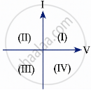
- For a solar-cell the I-V characteristics lies in the (IV) quadrant of the given graph.
- In a reverse biased p-n junction diode, the current measured in (μA), is due to majority charge carriers.
Consider the following statements A and B and identify the correct answer:
- For a solar-cell, the I-V characteristics lies in the IV quadrant of the given graph.
- In a reverse biased pn junction diode, the current measured in (A), is due to majority charge carriers.
