हिंदी
कर्नाटक बोर्ड पी.यू.सी.पीयूसी विज्ञान 2nd PUC Class 12

If the resistance R1 is increased (Figure), how will the readings of the ammeter and voltmeter change? - Physics

Advertisements
Advertisements

प्रश्न

If the resistance R1 is increased (Figure), how will the readings of the ammeter and voltmeter change?

टिप्पणी लिखिए
Advertisements

उत्तर

Let us redraw the circuit diagram to find the change in reading of the ammeter and voltmeter.

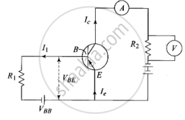
So, `I_BR_1 + V_(BE) = V_(BB)`

Base current, `I_B = (V_(BB) - V_(BE))/R_1`

`I_B ∝ 1/R_1`

So, R1 is increased, IB is decreased.

Now, the current in the ammeter is collector current IC.

IC = βIB as IB is decreased, IC is also decreased and the reading of the voltmeter and ammeter also decreased.

shaalaa.com
  क्या इस प्रश्न या उत्तर में कोई त्रुटि है?
अध्याय 14: Semiconductor Electronics - Exercises [पृष्ठ ९२]

APPEARS IN

एनसीईआरटी एक्झांप्लर Physics [English] Class 12
अध्याय 14 Semiconductor Electronics
Exercises | Q 14.25 | पृष्ठ ९२

वीडियो ट्यूटोरियलVIEW ALL [3]

संबंधित प्रश्न

Explain with the help of a diagram, how depletion region and potential barrier are formed in a junction diode.


A p-n photodiode is fabricated from a semiconductor with band gap of 2.8 eV. Can it detect a wavelength of 6000 nm?


Why is zener diode fabricated by heavily doping both p- and n-sides of the junction?


How is a photodiode fabricated?


The current in the forward bias is known to be more (~mA) than the current in the reverse bias (~μA). What is the reason, then, to operate the photodiode in reverse bias?


Draw the circuit diagram of a full wave rectifier using p-n junction diode.

Explain its working and show the output, input waveforms.


Describe briefly, with the help of a diagram, the role of the two important processes involved in the formation of a p-n junction.


Explain the formation of depletion layer and potential barrier in a p−n junction.


The plate resistance of a triode is 8 kΩ and the transconductance is 2.5 millimho. (a) If the plate voltage is increased by 48 V and the grid voltage is kept constant, what will be the increase in the plate current? (b) With plate voltage kept constant at this increased value, by how much should the grid voltage be decreased in order to bring the plate current back to its initial value?


Draw the circuit arrangement for studying the V-I characteristics of a p-n junction diode in reverse bias. Plot the V-I characteristics in this case.


What is a solar cell?


With reference to Semiconductor Physics,

Name the process that causes depletion region in a p-n junction.


Explain photodiode.


What is the magnitude of the potential barrier across a Ge p-n junction?


Which one of the following is not the advantage of LED?


Read the following paragraph and answer the questions.

LED is a heavily doped P-N junction which under forward bias emits spontaneous radiation. When it is forward-biased, due to recombination of holes and electrons at the junction, energy is released in the form of photons. In the case of Si and Ge diode, the energy released in recombination lies in the infrared region. LEDs that can emit red, yellow, orange, green and blue light are commercially available. The semiconductor used for fabrication of visible LEDs must at least have a band gap of 1.8 eV. The compound semiconductor Gallium Arsenide – Phosphide is used for making LEDs of different colours.


LEDs of different kinds

  1. Why are LEDs made of compound semiconductor and not of elemental semiconductors?
  2. What should be the order of bandgap of an LED, if it is required to emit light in the visible range?
  3. A student connects the blue coloured LED as shown in the figure. The LED did not glow when switch S is closed. Explain why?

    OR
    iii. Draw V-I characteristic of a p-n junction diode in
    (i) forward bias and (ii) reverse bias

Briefly explain how emf is generated in a solar cell.


Draw the circuit diagram of an illuminated photodiode and its I-V characteristics.


Share
Notifications

Englishहिंदीमराठी


      Forgot password?
Use app×