Advertisements
Advertisements
प्रश्न
(i) Explain with the help of a diagram the formation of depletion region and barrier potential in a pn junction.
Advertisements
उत्तर
(i) In a p−n junction, a p-type and an n-type material are joined together. The concentration of holes is higher in p-type material as compared to that in n-type material. Therefore, there is a concentration gradient between the p-type and n-type materials. As a result of this concentration gradient, holes move from p-side to n-side (p → n) by the process of diffusion. Similarly, electrons move from n-side to p-side (n → p).
As the holes diffuse from p-side, they leave ionised spaces (negatively charged) on p-side near the junction. These ionised spaces are immobile. Hence, a negative space-charge region is formed on the p-side near the junction. Similarly, a positive space-charge region is formed on the n-side. These two space-charge regions on either sides of the junction constitute what is called a depletion layer.
Since the n-side loses electrons and p-side gains electrons, a potential difference is developed across the junction of the two regions. This potential difference tends to oppose further motion of electrons from the n-region into the p-region. The same happens for holes too. The reverse polarity of this potential opposes further flow of carriers and is thus called the barrier potential

संबंधित प्रश्न
Explain the working of P-N junction diode in forward and reverse biased mode.
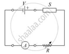
In the following diagram 'S' is a semiconductor. Would you increase or decrease the value of R to keep the reading of the ammeter A constant when S is heated? Give reason for your answer.
The graph shown in the figure represents a plot of current versus voltage for a given semiconductor. Identify the region, if any, over which the semiconductor has a negative resistance.

In a photo diode, the conductive increases when the material is exposed to light. It is found that the conductivity changes only if the wavelength is less than 620 nm. What is the band gap?
(Use Planck constant h = 4.14 × 10⁻¹⁵ eV-s, Boltzmann constant k = 8·62 × 10-5 eV/K.)
The dynamic plate resistance of a triode value is 10 kΩ. Find the change in the plate current if the plate voltage is changed from 200 V to 220 V.
Answer the following question.
Why photodiodes are required to operate in reverse bias? Explain.
Basic materials used in the present solid state electronic devices like diode, transistor, ICs, etc are ______.
In forward bias width of potential barrier in a p + n junction diode
Figure shows the transfer characteristics of a base biased CE transistor. Which of the following statements are true?

At Vi = 0.4 V, transistor is in active state.
At Vi = 1 V, it can be used as an amplifier.
At Vi = 0.5 V, it can be used as a switch turned off.
At Vi = 2.5 V, it can be used as a switch turned on.
A semiconductor device is connected in series with a battery, an ammeter and a resistor. A current flows in the circuit. If. the polarity of the battery is reversed, the current in the circuit almost becomes zero. The device is a/an ______.
